

High-speed digital signal integrated processing device for wireless communication
A high-speed digital signal and processing device technology, applied in the direction of electrical digital data processing, instruments, etc., can solve the problems that the speed cannot keep up, the high-speed modulation signal processing function cannot be realized, and the conversion accuracy cannot reach satisfactory accuracy. Effect of preventing signal crosstalk
- Summary
- Abstract
- Description
- Claims
- Application Information
AI Technical Summary
Problems solved by technology
Method used
Image

Examples
Embodiment Construction
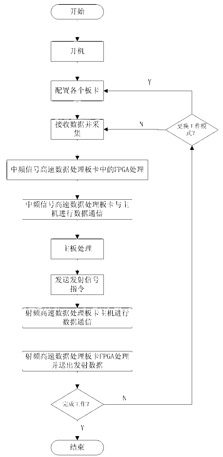
[0023] The present invention will be further described below in conjunction with the accompanying drawings and embodiments.
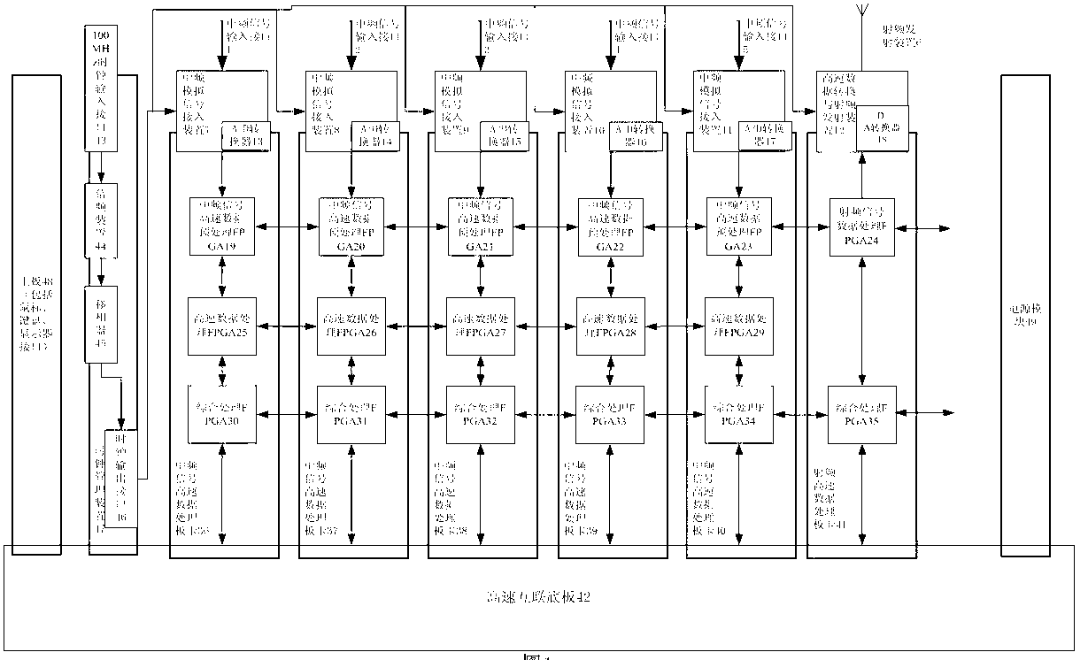
[0024] figure 1 It is a general structural block diagram of the high-speed digital signal integrated processing device for wireless communication of the present invention. The high-speed digital signal integrated processing device for wireless communication of the present invention includes a hardware part and control software, a clock management device 47, a main board 48, an intermediate frequency signal high-speed data processing board 36, and an intermediate frequency signal high-speed data processing board in the hardware part 37. An intermediate frequency signal high-speed data processing board 38, an intermediate frequency signal high-speed data processing board 39, an intermediate frequency signal high-speed data processing board 40, a radio frequency high-speed data processing board 41, and a power supply module 49 respectively communicate with...
PUM
 Abstract
Description
Claims
Application Information