Single even effect cross section obtaining method based on simulation

A single event effect and acquisition method technology, which is applied in the field of single event effect evaluation and simulation-based single event effect section acquisition, can solve the problem that the beam time cannot be guaranteed, the sensitive position of single event fault cannot be located, and the fault mechanism cannot be quantitatively analyzed Mechanism and other issues, to avoid model calibration problems, facilitate design improvement, and save test funds and time

Active Publication Date: 2013-03-27
NORTHWEST INST OF NUCLEAR TECH
View PDF4 Cites 33 Cited by
  • Summary
  • Abstract
  • Description
  • Claims
  • Application Information

AI Technical Summary

Problems solved by technology

The single event effect based on the ground simulation test depends on the limitation of domestic heavy ion sources, and the beam time cannot be guaranteed
At the same time, the evaluation of single event effects based on ground simulation e

Method used


Image

  • Single even effect cross section obtaining method based on simulation
  • Single even effect cross section obtaining method based on simulation
  • Single even effect cross section obtaining method based on simulation

Examples


Embodiment Construction

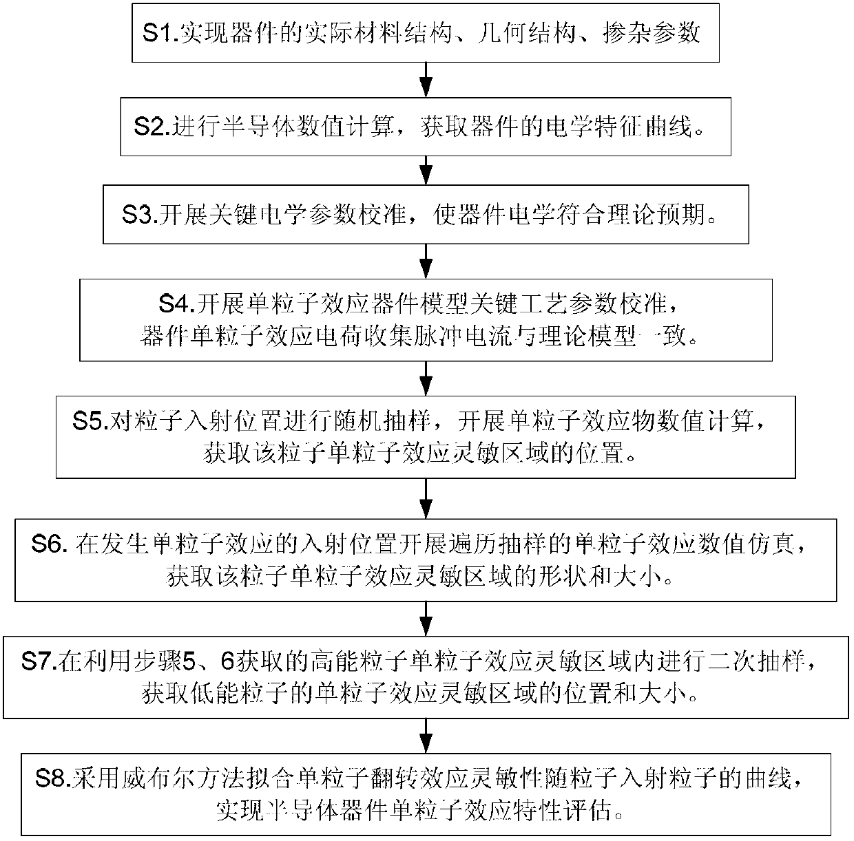
[0046] The invention provides a simulation-based acquisition method for the single event effect section, and realizes the theoretical evaluation of the single event effect.

[0047] figure 1 It is a flow chart of the simulation-based single event effect section acquisition method of the present invention.

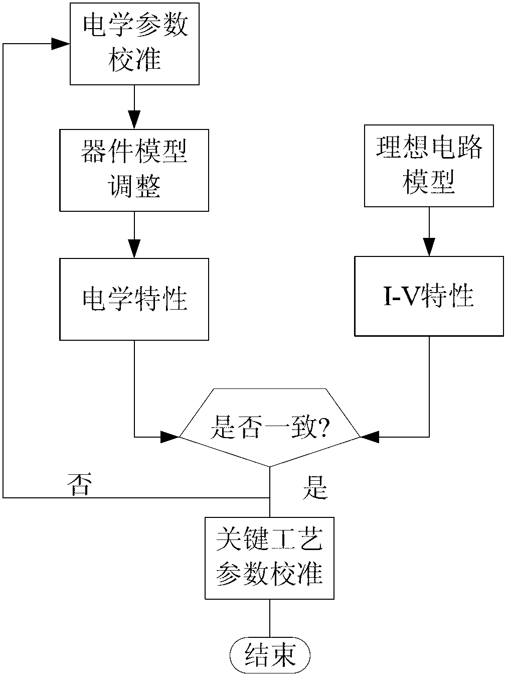
[0048] Step S1 realizes the actual material structure, geometric structure and doping parameters of the device, that is, the device model. There are two ways to establish the device structure. First, use a process simulation tool to generate the device. The method used for the influence of the process on the structure of the device. Second, with language-specific editing implementations, device editing requires artificial determination of device spatial dimensions and doping.

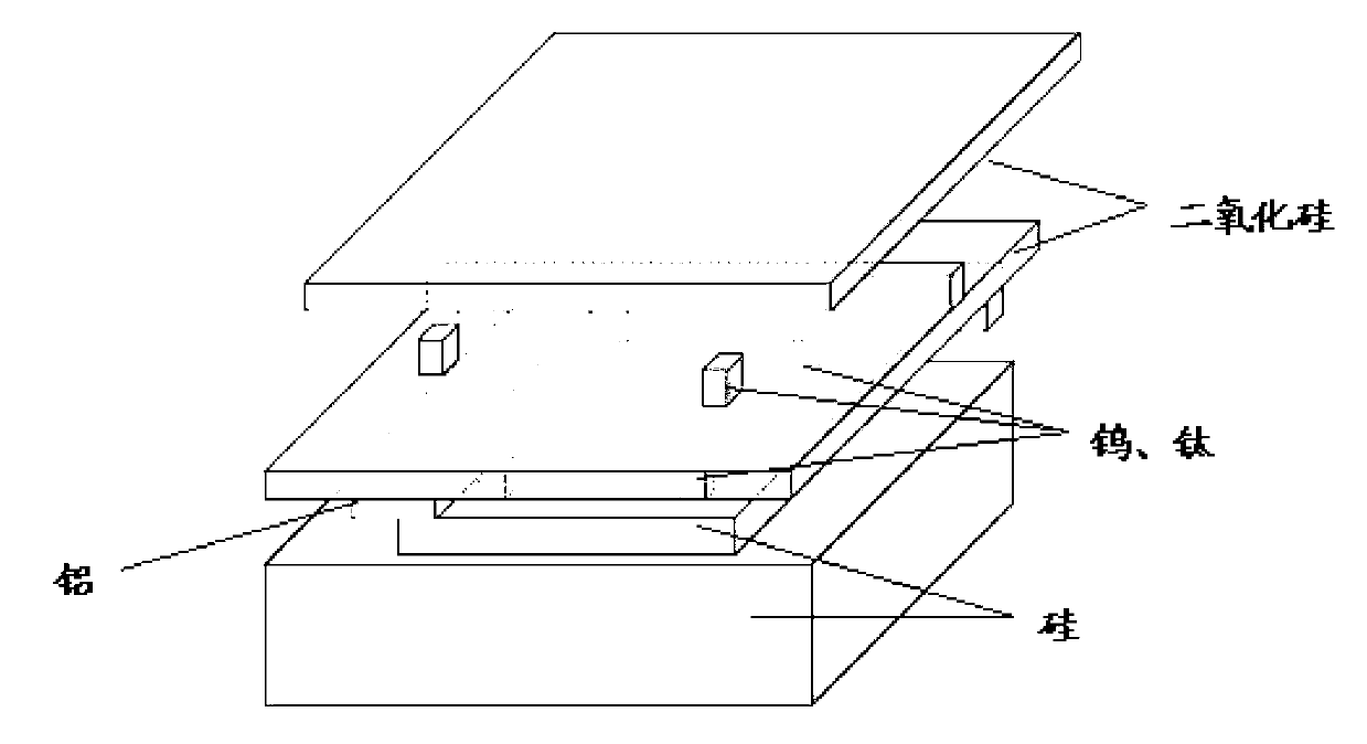
[0049] figure 2It is the present invention that builds a device model including material structure, geometry and doping parameters. The material structure is an important factor determining the ...


PUM


Abstract

The invention relates to a single even effect cross section obtaining method based on simulation. The single even effect cross section obtaining method comprises the following steps of: setting an actual material structure, geometric structure and doping parameters of a device, and realizing a complete device model; carrying out semiconductor characteristic numerical calculation, solving a diffusion drifting equation, a poisson equation and a current carrier continuity equation, and obtaining an electricity characteristic curve of the device; and calibrating key electrical parameters of a single even effect device model so that the device electricity is in line with theoretical expectation, wherein the key electricity parameters include a transistor transfer characteristic curve and a storage delay characteristic curve. The single even effect cross section obtaining method based on simulation, provided by the invention, has the advantages that the position of the single even effect error can be located, the relationship among the wiring and size of the device, the technological parameter of the device and the sensibility of the single event effect can be realized, and the confirmation of the single even effect performance can be realized in the design stage.

Description

technical field [0001] The invention relates to a single event effect evaluation method, in particular to a simulation-based single event effect section acquisition method, which belongs to the technical field of microelectronics and the field of anti-radiation reinforcement technology. Background technique [0002] With the continuous development of microelectronics technology, electronic automation design tools continue to mature and become one of the prerequisites for integrated circuit research and development. Among them, the simulation technology of integrated circuit manufacturing and processing is to establish a corresponding mathematical and physical model based on the actual manufacturing process, and integrate the simulation analysis of the process and the physical characteristics of the device. Process and device simulation technology has become the core means of IC manufacturing process analysis. [0003] The single event effect refers to the generation of elec...

Claims


Application Information

Patent Timeline
IPC IPC(8): G06F17/50
Inventor 郭红霞张科营罗尹虹赵雯闫逸华王园明张凤祁郭晓强丁李丽王忠明王燕萍
Owner NORTHWEST INST OF NUCLEAR TECH
Why Eureka
Try Eureka