Wafer-level package structure and production method thereof

A technology of wafer-level packaging and packaging structure, which is applied in semiconductor/solid-state device manufacturing, semiconductor/solid-state device parts, semiconductor devices, etc., and can solve problems such as sealing protection and unresolved chips

Active Publication Date: 2013-03-27
ALPHA & OMEGA SEMICON INT LP
View PDF7 Cites 46 Cited by
  • Summary
  • Abstract
  • Description
  • Claims
  • Application Information

AI Technical Summary

Problems solved by technology

Similarly, there are U.S. patents with patent numbers US6420244 and 6852607 respectively. These patent ...

Method used


Image

  • Wafer-level package structure and production method thereof
  • Wafer-level package structure and production method thereof
  • Wafer-level package structure and production method thereof

Examples


preparation example Construction

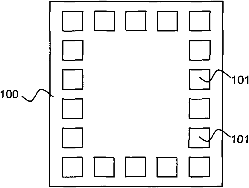
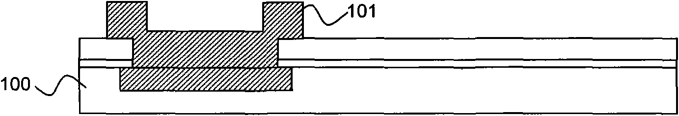
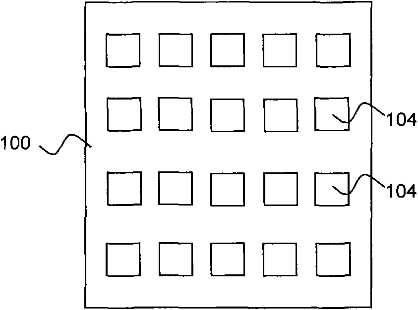
[0048] due to Figure 2J-2M In the shown manufacturing process, the substrate 200A included in the wafer 200 is cut into substrate units 200'A included in the chip 200', so for Figure 2MIn terms of the wafer-level packaging structure 200″A shown, in the silicon substrate unit 200′A included in the chip 200′, the metal material 208′ filled in the through hole 208 contacting the first type of arrangement pad 204a The first type of arrangement pad 204a in contact with the through hole 208 is electrically connected to the bottom electrode metal layer 209'. In an optional embodiment, the chip 200' is a MOSFET of vertical structure, that is, Its main current flows from the top of the device to the bottom, or vice versa. The drain region of the chip 200' is usually formed on the side near the bottom surface of the chip 200' in the substrate unit 200'A, in order to strengthen the contact between the bottom electrode metal layer 209' and the chip. 200' Ohmic contact of the drain regi...


PUM


Abstract

The invention relates to a semiconductor device package member and a production method thereof, in particular to a package structure and a production method thereof. In the package structure, a chip is packaged integrally without any parts exposed out of package compound in the wafer-level package structure. By the redistribution technology, welding pads distributed on the top surface of the chip are redistributed as array welding points in a top insulating dielectric layer covering the chip, and by through holes formed on a silicon substrate and metal materials filled in the through holes, some electrodes or signal terminals on the top plane of the chip are connected to a bottom electrode metal layer on the bottom plane of the chip. Besides, the chip can be sealed without seams by the top package member and the bottom package member included in the wafer-level package structure, and accordingly good mechanical protection and electrical protection are formed.

Description

technical field [0001] The present invention generally relates to a package body of a semiconductor device and a preparation method thereof, more precisely, the present invention relates to a method of packaging a chip as a whole in wafer-level packaging technology so that it is not exposed outside the plastic encapsulant Encapsulation structure and preparation method thereof. Background technique [0002] In the advanced chip packaging method, WLCSP (Wafer Level Chip Scale Packaging) is to package and test on the entire wafer first, and then plasticize it, and then cut it into individual IC packages particles, so the volume of the encapsulated package is almost equal to the original size of the bare chip, and the package has good heat dissipation and electrical performance. [0003] Usually, in the complex process flow of wafer-level packaging, whether it is based on the consideration of the reduction of substrate resistance or the reduction of chip size, it is ultimately ...

Claims


Application Information

Patent Timeline
IPC IPC(8): H01L21/56H01L21/78H01L23/31H01L23/00
CPCH01L24/94H01L2224/0401H01L2224/05554H01L2224/05558H01L2224/0557H01L2224/06181H01L2224/12105H01L2224/73253H01L2224/94H01L2924/00014H01L2924/13091H01L2924/181H01L2224/11H01L2224/03H01L2924/00H01L2224/05552
Inventor 薛彦迅黄平何约瑟哈姆扎·耶尔马兹鲁军鲁明联
Owner ALPHA & OMEGA SEMICON INT LP
Why Eureka
Try Eureka