Method for flip integration of array beam guide grate chip and semiconductor optical amplifier chip

A technology of arrayed waveguide gratings and optical amplifiers, applied in semiconductor lasers, optical waveguides, lasers, etc., can solve the problems of complex process flow and high cost, and achieve the effects of simplifying the integration process, improving reliability, and improving integration efficiency

Inactive Publication Date: 2013-03-27
GUANGXUN SCI & TECH WUHAN
View PDF3 Cites 21 Cited by
  • Summary
  • Abstract
  • Description
  • Claims
  • Application Information

AI Technical Summary

Problems solved by technology

For the hybrid integration method of AWG chips and SOA chips, a common way in current reports is to respectively fix the two chips on the same prefabricated substrate or substrate to achieve passive alignment. This method is costly , the process is more complex

Method used


Image

  • Method for flip integration of array beam guide grate chip and semiconductor optical amplifier chip
  • Method for flip integration of array beam guide grate chip and semiconductor optical amplifier chip
  • Method for flip integration of array beam guide grate chip and semiconductor optical amplifier chip

Examples


Embodiment Construction

[0034] Further detailed description will be made below in conjunction with specific embodiments and with reference to the accompanying drawings.

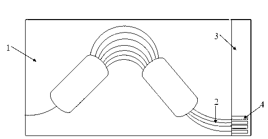
[0035] The method for flip-chip integrating silicon-based silicon dioxide AWG chips and SOA chips provided by the present invention, the working principle of the present invention is to firstly design and manufacture a silicon-based silicon dioxide AWG chip suitable for this integration, and then sequentially integrate the silicon-based silicon dioxide AWG chip on the AWG chip The positioning area, alignment marks and electrodes are made, and finally the SOA chip is aligned and flip-chip integrated on the AWG chip.

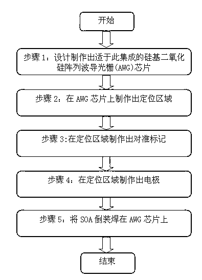
[0036] Such as figure 1 as shown, figure 1 It is a flow chart of the method for flip-chip integrating silicon-based silicon dioxide AWG chips and SOA chips provided by the present invention, including the following steps:

[0037] Step 1: Design and manufacture an AWG chip suitable for integration

[0038] The specif...


PUM


Abstract

The invention discloses a method for flip integration of an array beam guide grate chip and a semiconductor optical amplifier chip. The method comprises steps of designing and producing the array beam guide grate chip which is suitable to integration; producing a positioning region on the array beam guide grate chip; producing an aligning mark in the positioning region of the array beam guide grate chip; producing an electrode in the positioning region of the array beam guide grate chip; and welding the semiconductor optical amplifier chip to the positioning region of the array beam guide grate chip in a flip mode after aligning the aligning mark of the semiconductor optical amplifier chip to the aligning mark of the positioning region. By the aid of the method, a semiconductor optical amplifier (SOA) chip can be integrated to the substrate of an Arrayed Waveguide Grating (AWG), the reliability of the device is improved, the integration process is simplified and the integration effectively is improved.

Description

[0001] technical field [0002] The invention relates to a process method for hybrid integration of active devices and passive devices, in particular to a method for flip-chip integration of arrayed waveguide grating (AWG Arrayed Waveguide Grating) chips and semiconductor optical amplifier (SOA Semiconductor Optical Amplifier) ​​chips. The invention belongs to communication field. [0003] Background technique [0004] In wavelength division multiplexing (WDM) systems, multi-wavelength lasers and tunable lasers play an extremely important role. In various forms of multi-wavelength or tunable semiconductor lasers, the arrayed waveguide grating of silicon-based silicon dioxide material is integrated with several semiconductor optical amplifiers, the AWG is used as a resonant cavity, and the semiconductor optical amplifier is used as a light source. Realize the plan. This scheme has many advantages. First, it can continuously and efficiently output optical signals of all spe...

Claims


Application Information

Patent Timeline
Patent Type & Authority Applications(China)
IPC IPC(8): H01S5/026H01S5/12G02B6/13
Inventor 马卫东丁丽李迪赵建宜朱虎陈昊王宁
Owner GUANGXUN SCI & TECH WUHAN
Why Eureka
Try Eureka