Real-time temperature, optical band gap, film thickness, and surface roughness measurement for thin films applied to transparent substrates

A technology for surface roughness, transparent substrates, applied in the direction of using optical devices, measuring devices, scattering characteristics measurement, etc., can solve problems such as inability to obtain stable or reliable results

Inactive Publication Date: 2013-03-27
K SPACE ASSOCS
View PDF7 Cites 15 Cited by
  • Summary
  • Abstract
  • Description
  • Claims
  • Application Information

AI Technical Summary

Problems solved by technology

However, these prior art techniques are based on certain analytical methods that do not yield stable or reliable results

Method used


Image

  • Real-time temperature, optical band gap, film thickness, and surface roughness measurement for thin films applied to transparent substrates
  • Real-time temperature, optical band gap, film thickness, and surface roughness measurement for thin films applied to transparent substrates
  • Real-time temperature, optical band gap, film thickness, and surface roughness measurement for thin films applied to transparent substrates

Examples


Embodiment Construction

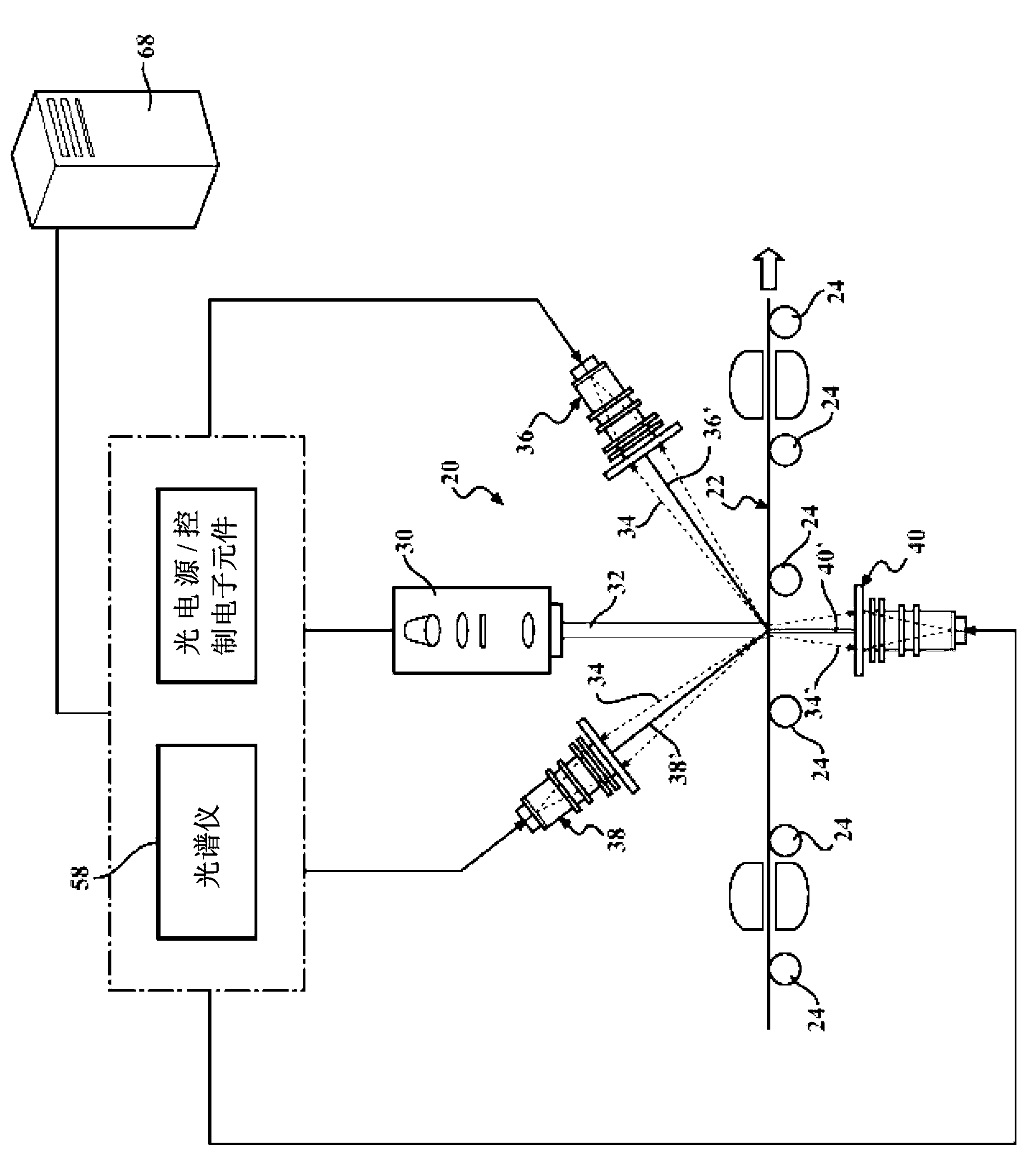
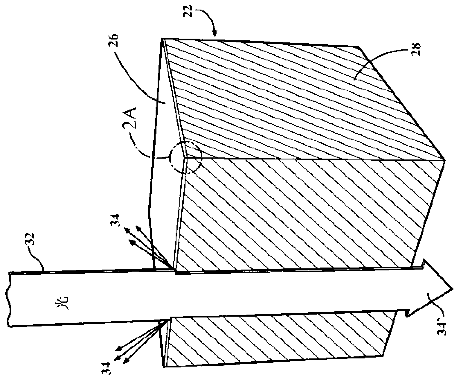
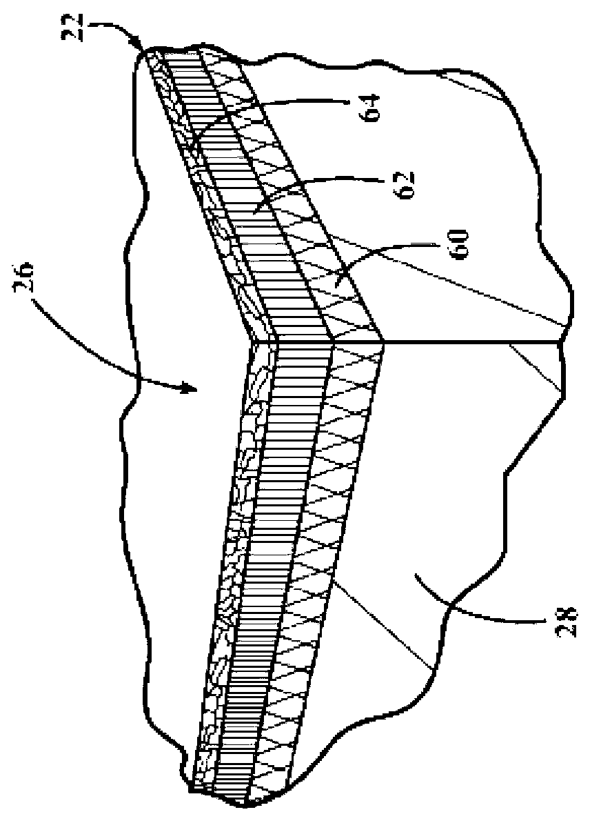
[0036] Referring to the drawings, wherein like reference numerals are used to indicate like or corresponding parts in the various views, an absorption edge measurement system according to the present invention is shown generally at 20 . The system 20 is particularly suited for in-line measurement of material 22 moving along a conveyor system 24 . Typical materials 22 include the production of photovoltaic solar panels on which a thin film absorber layer 26 is applied across a glass (or other suitable) substrate 28 . Substrate 28 and membrane 26 are shown schematically in Figures 2, 2A, 3A and 3B. It should be understood that film 26 may actually consist of multiple discrete layers, as shown in FIG. 2A. The thin film component 26 can be any typical material, including but not limited to CdTe, CIGS, CdS, textured polysilicon, GaAs, Si, SiC, InP, ZnSe, ZnTe, SrTi. 3 and GaN.

[0037] In the particular example of a photovoltaic panel product, in which the materials 22 comprise ...


PUM

PropertyMeasurementUnit
thicknessaaaaaaaaaa

Abstract

A method and apparatus (20) used in connection with the manufacture of thin film semiconductor materials (26) deposited on generally transparent substrates (28), such as photovoltaic cells, for monitoring a property of the thin film (26), such as its temperature, surface roughness, thickness and / or optical absorption properties. A spectral curve (44) derived from diffusely scattered light (34, 34') emanating from the film (26) reveals a characteristic optical absorption (Urbach) edge. Among other things, the absorption edge is useful to assess relative surface roughness conditions between discrete material samples (22) or different locations within the same material sample (22). By comparing the absorption edge qualities of two or more spectral curves, a qualitative assessment can be made to determine whether the surface roughness of the film (26) may be considered of good or poor quality.

Description

[0001] Cross References to Related Applications [0002] This application claims priority to US Provisional Application No. 61 / 362,938, filed July 9, 2010, which is hereby incorporated by reference in its entirety. technical field [0003] The present invention generally relates to non-contact measurement of thin film layers applied to substantially transparent substrates; more particularly for evaluating at least the relative surface roughness of thin films with reference to the optical absorption edge of the thin film material. Background technique [0004] Advanced manufacturing processes involving the deposition of thin films on substrates often rely on the ability to monitor semiconductor material properties such as its temperature, surface roughness, thickness and / or optical absorption properties with high precision and repeatability. [0005] As is currently known, when the photon energy exceeds the bandgap energy, a sudden strong absorption will occur. In "A New Op...

Claims


Application Information

Patent Timeline
Patent Type & Authority Applications(China)
IPC IPC(8): G01B11/30G01N21/958
CPCG01N21/8422G01B11/0625G01B11/303G01B11/0616G01N21/47G01B11/30G01N21/958
Inventor 达里尔·巴利特查尔斯·A·泰勒二世巴里·D·维斯曼
Owner K SPACE ASSOCS
Why Eureka
Try Eureka