Silicon waveguide refractive index calorescence adjusting structure

A refractive index, light adjustment technology, applied in optics, nonlinear optics, instruments, etc., can solve the problems of slow speed, limited adjustment range, large adjustment power consumption, etc., to achieve large adjustment range, short response time, and adjustment power consumption. low effect

Inactive Publication Date: 2013-04-03
SHANGHAI JIAO TONG UNIV
View PDF5 Cites 21 Cited by
  • Summary
  • Abstract
  • Description
  • Claims
  • Application Information

AI Technical Summary

Problems solved by technology

[0004] Based on the reported methods, the electrical adjustment structure using the carrier dispersion effect is faster, but the adjustment range is limited, and absorption loss will be introduced at the same time. This method is suitable for modulators, and for devices

Method used


Image

  • Silicon waveguide refractive index calorescence adjusting structure
  • Silicon waveguide refractive index calorescence adjusting structure
  • Silicon waveguide refractive index calorescence adjusting structure

Examples


Embodiment

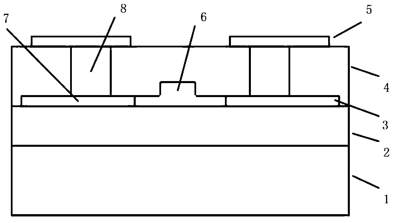
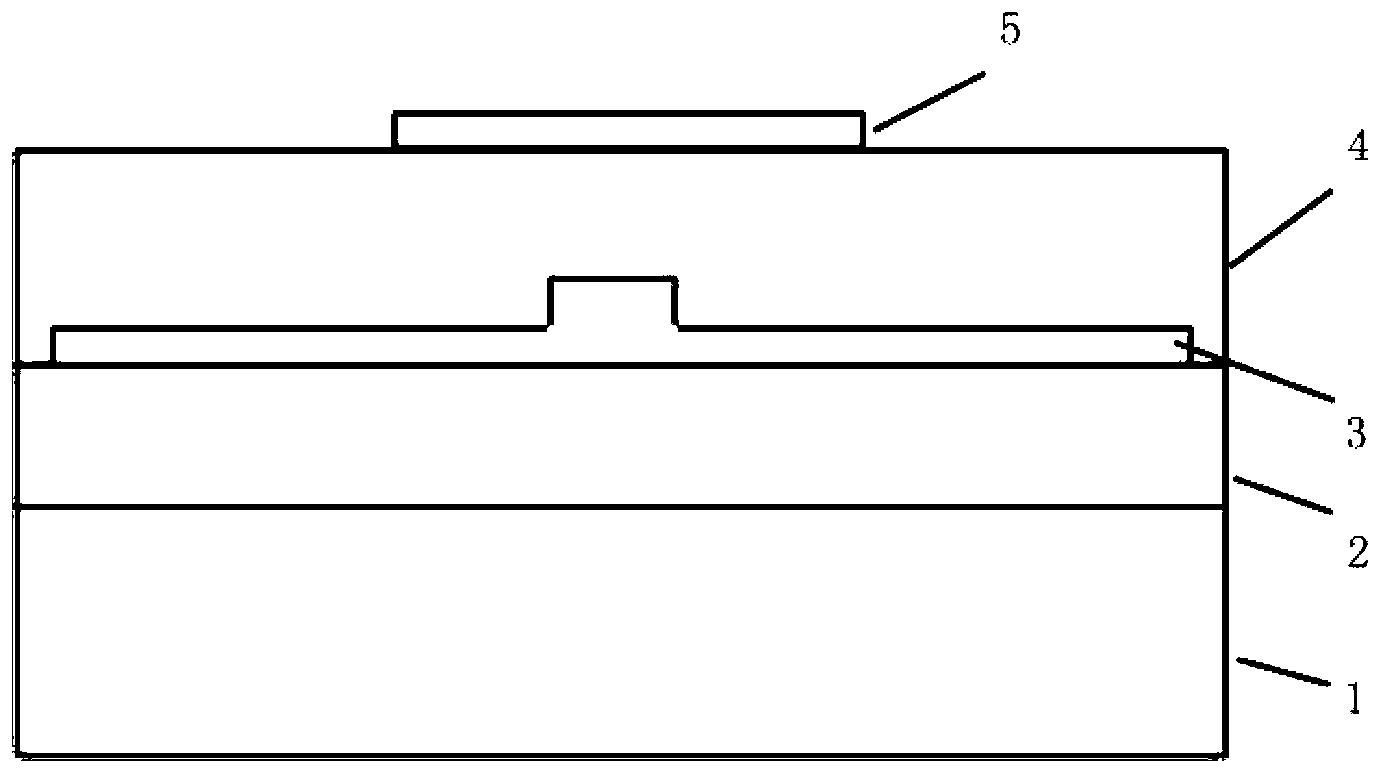
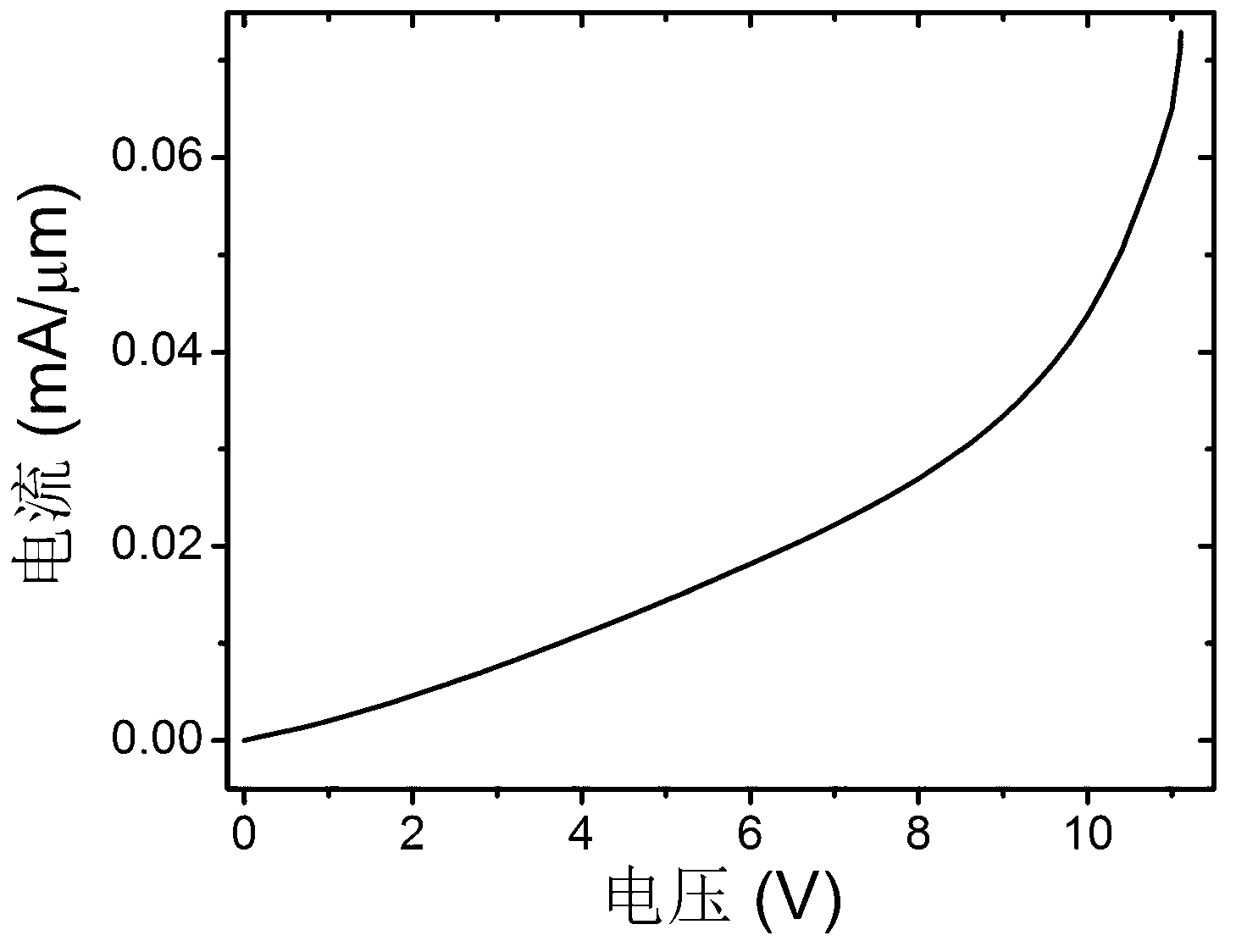
[0032] In this embodiment, the thickness of the lower cladding layer 2 is 2 μm; the width of the ridge of the waveguide layer 3 is 500 nm, the height of the inner ridge is 220 nm, and the height of the outer ridge is 60 nm; the thickness of the upper cladding layer 4 is 1.5 μm. The heavily doped region 7 is p-type doped with a width of 4μm and a doping concentration of 10 20 cm -3 ; Lightly doped intrinsic i-region 6 doping concentration 10 15 cm -3 The edge of the heavily doped region 7 is separated from the edge of the waveguide core region by 300 nm; the width of the through hole is 1 μm; a p-i-p thermal resistance structure is formed. The relationship between voltage and current of this p-i-p thermal resistance structure is as image 3 As shown, after the voltage increased to ~9.5V, the resistance continued to decrease as the voltage increased. When an external voltage of 4V is applied, the temperature distribution diagram of the structure after stabilization is as follows ...


PUM


Abstract

The invention discloses a silicon waveguide refractive index calorescence adjusting structure, which sequentially comprises a substrate, a lower cladding, a waveguide layer, an upper cladding and an electrode layer from bottom to top; the waveguide layer is in a ridge shape, a central area of the ridge shape is a lightly-doped intrinsic area I, and flat areas on two sides of the ridge shape are respectively heavily-doped areas; and two sides of the upper cladding are respectively provided with a metal through hole, and the heavily-doped areas of the waveguide layer are connected with the electrode layer through the through hole. After an external power supply is electrified, the waveguide layer produces heat, the temperature in a waveguide core area is increased, and the refractive index is increased, so that the calorescence adjusting effect is realized. The waveguide layer is used as hot resistance to produce the heat, and the heat source directly acts on a light field, so that compared with a traditional calorescence adjusting structure adopting a metal resistance, the silicon waveguide refractive index calorescence adjusting structure has characteristics of lower power consumption and shorter response time.

Description

Technical field [0001] The invention relates to a silicon waveguide refractive index thermo-optical adjustment structure, which belongs to the field of integrated optoelectronics. Background technique [0002] In recent years, integrated optoelectronic technology has developed rapidly, the size of devices has become smaller and the integration of chips has become higher and higher, and the cross-sectional size of optical waveguides has been reduced to the sub-micron scale. Due to the high refractive index difference between silicon material and air and silicon dioxide, it has strong light confinement ability and is easy to produce sub-micron optical waveguide devices; its production process is compatible with microelectronic integrated circuit technology, which greatly reduces It reduces the cost and facilitates the realization of photoelectric integration, making it one of the most competitive materials for photoelectric integrated chips. Many passive and active integrated opto...

Claims


Application Information

Patent Timeline
IPC IPC(8): G02F1/015G02F1/01
Inventor 陆梁军周林杰谢静雅邹志孙晓萌李新碗陈建平
Owner SHANGHAI JIAO TONG UNIV
Why Eureka
Try Eureka