Semiconductor chip and manufacturing method thereof
A semiconductor and wafer technology, applied in the field of semiconductor wafers and their preparation, can solve the problems of affecting the shape of a columnar semiconductor structure, affecting the withstand voltage characteristics and reliability of the wafer, etc., and achieve the effects of compact product structure, reduced production cost, and simple production process
- Summary
- Abstract
- Description
- Claims
- Application Information
AI Technical Summary
Problems solved by technology
Method used
Image

Examples
Embodiment
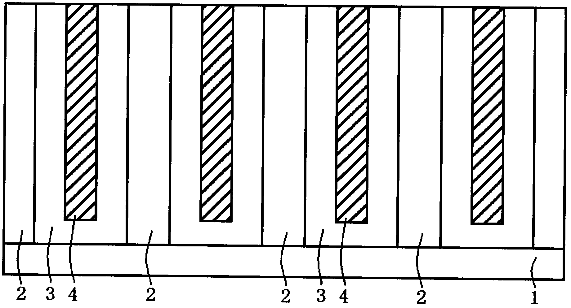
[0021] figure 1 It is a schematic cross-sectional view of a semiconductor wafer of the present invention, combined below figure 1 The semiconductor device of the present invention will be described in detail.
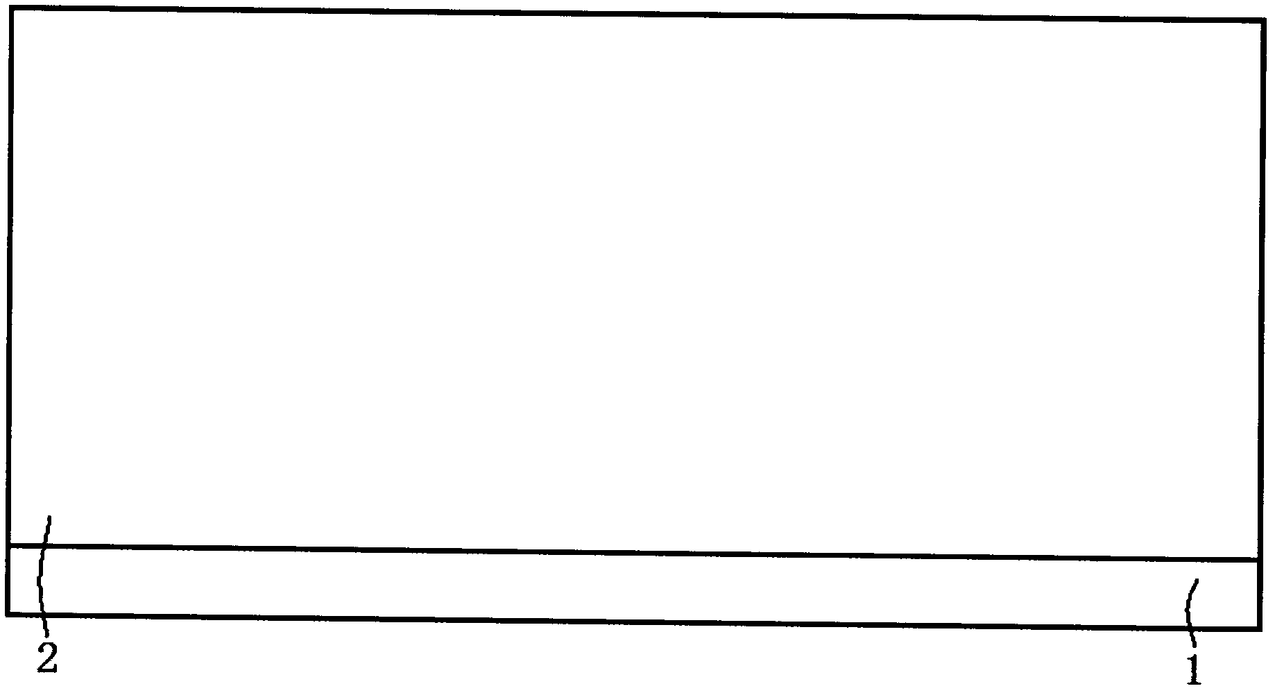
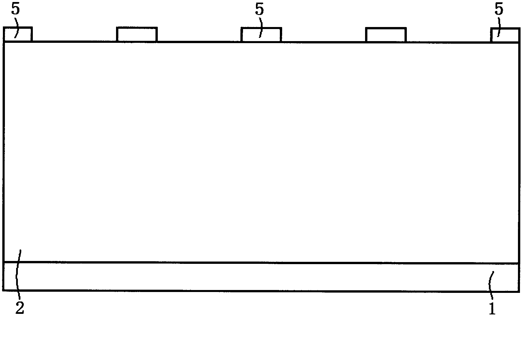
[0022] A semiconductor wafer with a super junction structure, comprising: a substrate layer 1, which is a semiconductor silicon material of N conductivity type, and the doping concentration of phosphorus atoms is 1E20cm-3; a first semiconductor layer 2, which is located on the substrate layer 1, is N Conductive type semiconductor silicon material with a width of 4 μm, a thickness of 20 μm, and a doping concentration of phosphorus atoms of 1E16 cm-3; the second semiconductor layer 3, located on the sidewall of the first semiconductor layer 2 and the surface of the substrate layer 1, is of P conductivity type The semiconductor silicon material has a width of 2 μm and a thickness of 20 μm, and the doping concentration of boron atoms is 1E16 cm −3 ; the insulating layer 4 ...
PUM
 Abstract
Description
Claims
Application Information