Schottky contact groove type power diode and preparation method thereof
A Schottky contact and power diode technology, which is applied in semiconductor/solid-state device manufacturing, electrical components, circuits, etc., can solve the problems of sacrificing device on-resistance and chip area utilization, and achieve low on-resistance and small leakage Current, the effect of good reverse withstand voltage characteristics
- Summary
- Abstract
- Description
- Claims
- Application Information
AI Technical Summary
Problems solved by technology
Method used
Image

Examples
Embodiment 1
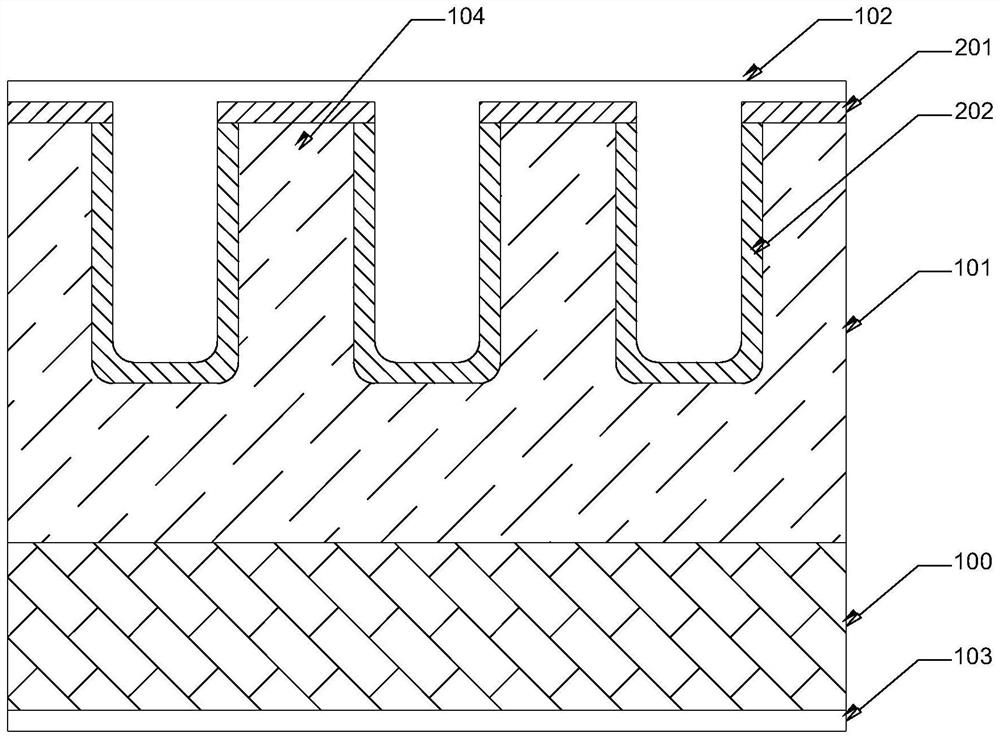
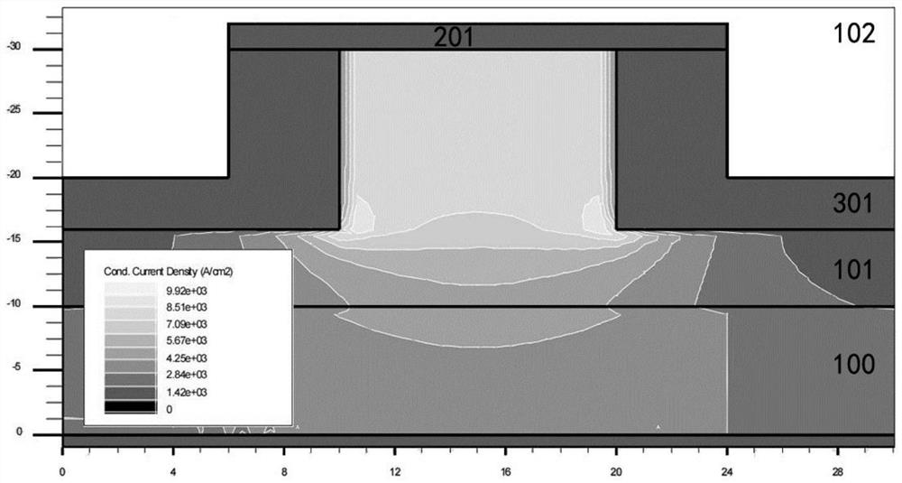
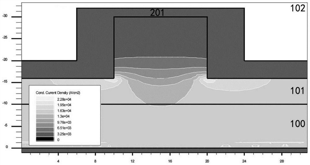
[0046] Such as figure 1 As shown, a Schottky-contact trench power diode of the present invention includes an n-type drift layer 101 , an n-type substrate 100 and a lower electrode 103 stacked sequentially from top to bottom. Several ribs 104 extend upward from the upper end of the n-type drift layer 101 , and grooves are formed between the ribs 104 . A high barrier layer 202 is laid in the trench, and the high barrier layer 202 is in Schottky contact with the n-type drift layer 101 . A low barrier layer 201 is laid on the rib 104 to cover the upper end surface of the rib 104 and the end of the high barrier layer 202 , and the low barrier layer 201 and the n-type drift layer 101 are also in Schottky contact. The upper electrode 102 is set to fill and cover the surfaces of the high barrier layer 202 and the low barrier layer 201 .
[0047] In this embodiment, the n-type drift layer 101 is made of gallium oxide, and the n-type substrate 100 is also made of gallium oxide, but th...
Embodiment 2
[0068] Such as Figure 9 As shown, compared with Embodiment 1, the structural difference is mainly that an insulating dielectric layer 203 is provided at the corner of the groove bottom and the rib 104 to alleviate the electric field concentration effect: the electric field has a maximum value at the corner of the groove bottom and the rib 104, and by introducing The insulating dielectric layer optimizes the distribution of the electric field and reduces the value of the electric field at the corner, thereby improving the breakdown characteristics of the device. The insulating dielectric layer 203 is located between the high barrier layer 202 and the n-type drift layer 101 , disconnecting the electrical contact there.
[0069] The preparation method is also adjusted on the basis of Example 1: before depositing the high barrier layer 202, first deposit the insulating dielectric layer 203 at the bottom of the trench, and make the insulating dielectric layer 203 cover the lower e...
Embodiment 3
[0071] Such as Figure 10 As shown, corresponding to the second embodiment, the structural difference mainly lies in that the insulating dielectric layer 203 covers the bottom of the trench entirely except for the corners. The electrical contact between the high barrier layer 202 at the lower part of the trench and the n-type drift layer 101 is completely disconnected.
[0072] Compared with the second embodiment, the preparation method is all about covering the bottom and corners of the trench when depositing the insulating dielectric layer 203 .
[0073] Compared with Embodiment 2, Embodiment 3 sacrifices part of the conduction area, but there is one less etching step in the preparation process, which reduces the cost, and the insulating dielectric layer in the two device structures has played a role in alleviating the electric field concentration effect and improving The effect of device breakdown characteristics, other electrical characteristics are not significantly diff...
PUM
| Property | Measurement | Unit |
|---|---|---|
| Work function | aaaaa | aaaaa |
| Thickness | aaaaa | aaaaa |
| Thickness | aaaaa | aaaaa |
Abstract
Description
Claims
Application Information