Supercharge Your Innovation With Domain-Expert AI Agents!

Super junction structure semiconductor wafer with insulating layer isolation and preparation method thereof

A semiconductor and insulating layer technology, applied in the field of superjunction semiconductor wafers, can solve the problems affecting the shape of the columnar semiconductor structure, affecting the withstand voltage characteristics and reliability of the wafer, etc., and achieve the effects of compact product structure, lower resistance, and lower production costs.

Inactive Publication Date: 2013-06-05
朱江 +1
View PDF7 Cites 0 Cited by
  • Summary
  • Abstract
  • Description
  • Claims
  • Application Information

AI Technical Summary

Problems solved by technology

The manufacturing process of semiconductor wafers with such a super-junction structure requires multiple anisotropic dry etching processes to control the distribution of columnar P-type semiconductors and N-type semiconductor regions, which easily affects the shape of the columnar semiconductor structure, thereby affecting the withstand voltage characteristics of the wafer. and reliability

Method used


Image

  • Super junction structure semiconductor wafer with insulating layer isolation and preparation method thereof
  • Super junction structure semiconductor wafer with insulating layer isolation and preparation method thereof
  • Super junction structure semiconductor wafer with insulating layer isolation and preparation method thereof

Examples


Embodiment 1

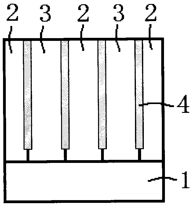
[0030] figure 1 It is a schematic cross-sectional view of a semiconductor wafer with an insulating layer-isolated superjunction structure of the present invention, combined below figure 1 The semiconductor device of the present invention will be described in detail.

[0031] A semiconductor wafer with a super junction structure isolated by an insulating layer, comprising: a substrate layer 1, which is an N conductivity type semiconductor silicon material, and the doping concentration of phosphorus atoms is 1E20cm -3 ; N-type semiconductor silicon material 2, located on the substrate layer 1, is an N-type semiconductor silicon material with a width of 2 μm and a thickness of 10 μm, and the doping concentration of phosphorus atoms is 1E16cm -3 ; The P-type semiconductor silicon material 3, located between the N-type semiconductor silicon materials 2, is an N-conduction type semiconductor silicon material with a width of 2 μm and a thickness of 10 μm, and the doping concentratio...

Embodiment 2

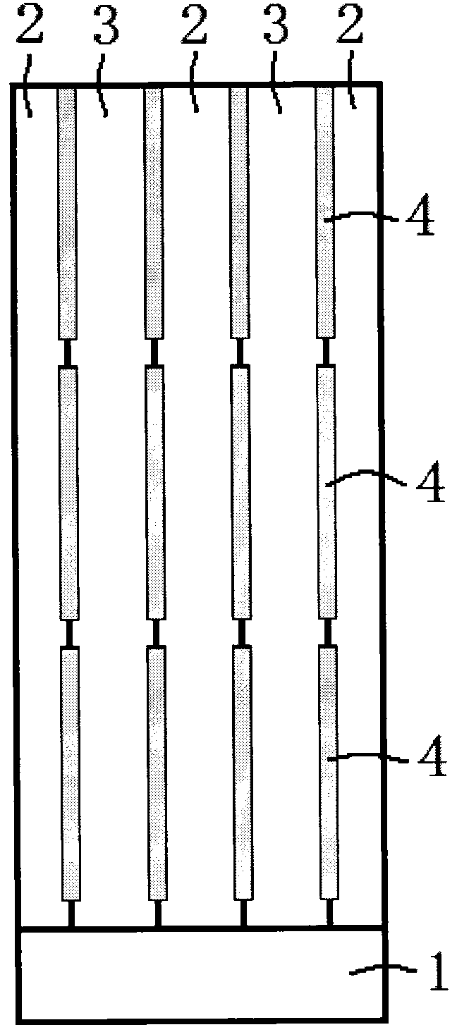
[0040] figure 2 It is a schematic cross-sectional view of a semiconductor wafer with an insulating layer-isolated superjunction structure of the present invention, combined below figure 2 The semiconductor device of the present invention will be described in detail.

[0041] A semiconductor wafer with a super junction structure isolated by an insulating layer, comprising: a substrate layer 1, which is an N conductivity type semiconductor silicon material, and the doping concentration of phosphorus atoms is 1E20cm -3 ; N-type semiconductor silicon material 2, located on the substrate layer 1, is an N-conduction type semiconductor silicon material with a width of 2 μm and a thickness of 30 μm, and the doping concentration of phosphorus atoms is 1E16cm -3 ; The P-type semiconductor silicon material 3, located between the N-type semiconductor silicon materials 2, is an N-conduction type semiconductor silicon material with a width of 2 μm and a thickness of 30 μm, and the doping...


PUM


Abstract

The invention discloses a super junction structure semiconductor wafer with insulating layer isolation and a preparation method thereof. Technically, columnar structures of P-type semiconductor and N-type semiconductor regions are easy to control, and an ideal structure perpendicular to the semiconductor wafer is easy to form on junction faces and isolation faces of PN junctions, so that an electric field can be expanded ideally and uniformly in depletion layers when reverse bias voltages are imposed and charges complement mutually, and the electrical parameter property and the reliability of an apparatus are improved.

Description

technical field [0001] The invention relates to a super junction structure semiconductor wafer with insulating layer isolation, and also relates to a preparation method of the super junction structure semiconductor wafer with insulating layer isolation. Background technique [0002] The semiconductor wafer structure capable of achieving high withstand voltage and low on-resistance is a structure in which columnar P-type semiconductors and N-type semiconductor regions are alternately arranged side by side, and the columnar P-type semiconductors and N-type semiconductors are perpendicular to the wafer surface. By setting the impurity concentration and width of the P-type semiconductor and the N-type semiconductor to desired values, a high breakdown voltage can be realized when a reverse voltage drop is applied. Such a structure is called a superjunction structure. [0003] Known super junction structure semiconductor wafer structure and manufacturing method are as follows: ...

Claims


Application Information

Patent Timeline
Patent Type & Authority Applications(China)
IPC IPC(8): H01L29/78H01L29/06H01L21/336
Inventor 朱江盛况
Owner 朱江
Features
  • R&D
  • Intellectual Property
  • Life Sciences
  • Materials
  • Tech Scout
  • Unparalleled Data Quality
  • Higher Quality Content
  • 60% Fewer Hallucinations
Learn More