

Light emitting diode and production method thereof
A technology for light-emitting diodes and a manufacturing method, which is applied to vacuum evaporation plating, coatings, semiconductor devices, etc., can solve problems such as process parameter adjustment and difficulty, and achieve the effects of ensuring stress release, ensuring adhesion, and improving light extraction efficiency.
Active Publication Date: 2013-04-03
ANHUI SANAN OPTOELECTRONICS CO LTD
View PDF4 Cites 19 Cited by
- Summary
- Abstract
- Description
- Claims
- Application Information
AI Technical Summary
Problems solved by technology
Method used
View moreImage
Smart ImageViewing Examples

Examples
Embodiment 1
Embodiment 2
Login to View More PUM
| Property | Measurement | Unit |
|---|---|---|
| electrical conductor | aaaaa | aaaaa |
Abstract
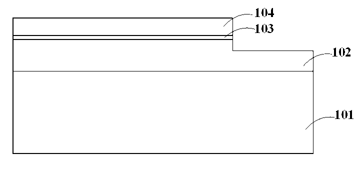
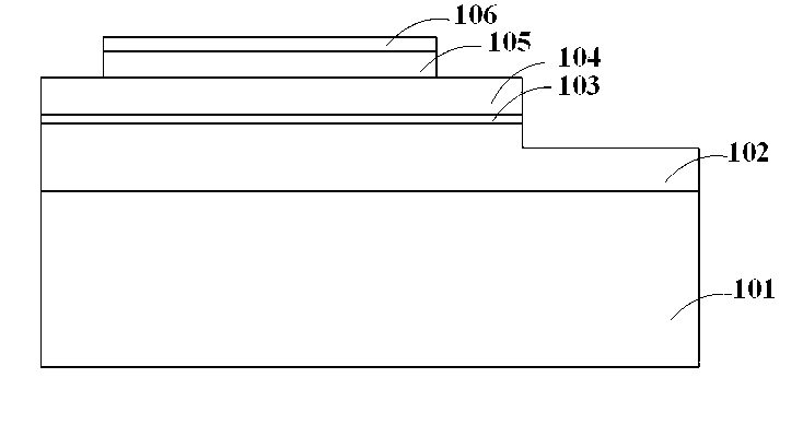
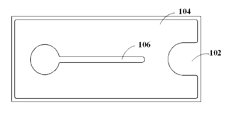
The invention discloses a light emitting diode (LED) with a transparent conducting layer and a production method thereof. The LED comprises a substrate; a luminous epitaxial layer which is formed by sequentially stacking a first limit layer, a luminous layer and a semiconducting material layer of a second limit layer from the bottom up, and is formed above the substrate; a current barrier layer which is formed above a local area of the luminous epitaxial layer; a transparent conducting structure which is formed above the current barrier layer, extends out of the surface of the luminous epitaxial layer and is divided into a luminous zone and a non-luminous zone; and an electrode P which is formed above the non-luminous zone of the transparent conducting structure, wherein the non-luminous zone is corresponding to the current barrier layer, the thickness of the non-luminous zone is larger than that of the luminous zone, and therefore the transparent conducting structure is enabled to form good ohmic contact with the luminous epitaxial layer, and decreases absorption of light. The structure can guarantee current expansibility, reduce working voltage, and decrease the absorption of the light.
Description
technical field [0001] The invention relates to a light-emitting diode and a manufacturing method thereof, more particularly to a light-emitting diode with a transparent conductive layer and a manufacturing method thereof. Background technique [0002] After years of development, light-emitting diodes (LEDs) have been widely used in different fields such as display, indication, backlight, and lighting. Group III-V compounds are currently the mainstream semiconductor materials for making light-emitting diodes, among which gallium nitride-based materials and aluminum gallium indium phosphide-based materials are the most common. The current spreading performance of traditional p-type III-V semiconductor materials is generally poor. In order to allow the current to be uniformly injected into the light-emitting layer, it is often necessary to add a transparent conductive layer on the p-type material layer. Among many materials that can be used as transparent conductive layers, s...
Claims
Login to View More Application Information
Patent Timeline
 Patent Type & AuthorityApplications(China)
IPC IPC(8): H01L33/38H01L33/00
CPCH01L33/38H01L2933/0016C23C14/086C23C14/24C23C14/5806C23C14/024C23C14/35H01L33/42C23C14/58H01L33/005H01L2933/0025H01L2933/0066
Inventor尹灵峰林素慧郑建森洪灵愿刘传桂欧毅德陈功
OwnerANHUI SANAN OPTOELECTRONICS CO LTD