Light emitting diode and production method thereof

A technology of light-emitting diodes and manufacturing methods, which is applied in the direction of vacuum evaporation plating, coating, semiconductor devices, etc., can solve problems such as difficulties and adjustment of process parameters, and achieve the effects of ensuring adhesion, ensuring stress release, and reducing ohmic contact

Active Publication Date: 2015-05-06
ANHUI SANAN OPTOELECTRONICS CO LTD
View PDF4 Cites 0 Cited by
  • Summary
  • Abstract
  • Description
  • Claims
  • Application Information

AI Technical Summary

Problems solved by technology

To adjust the process parameters of the coating, generally use segmented coating or reduce the rate, etc., and often have to take into account the photoelectric parameters and electrode adhesion, making it difficult to adjust the process parameters

Method used


Image

  • Light emitting diode and production method thereof
  • Light emitting diode and production method thereof
  • Light emitting diode and production method thereof

Examples


Embodiment 1

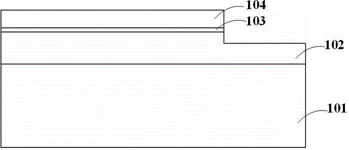
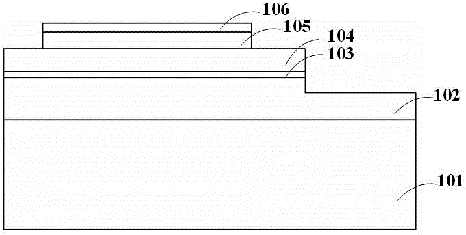
[0037] Such as Figure 6 As shown, a light-emitting diode device with a transparent conductive layer includes: a substrate 101; a light-emitting epitaxial layer, which is stacked from bottom to top with semiconductor material layers of a first confinement layer 102, a light-emitting layer 103 and a second confinement layer 104 formed on the substrate 101; the current blocking layer 105 is formed on the partial area of ​​the second confinement layer 104 of the light-emitting epitaxial layer; the first transparent conductive layer 106 is formed on the current blocking layer 105 , and the contact area between the first transparent conductive layer 106 and the current blocking layer 105 is equal to the upper surface area of ​​the current blocking layer 105; the second transparent conductive layer 107 is coated on the first transparent conductive layer 106 and the current blocking layer 105 and extend to the surface of the second confinement layer 104 of the light-emitting epitaxia...

Embodiment 2

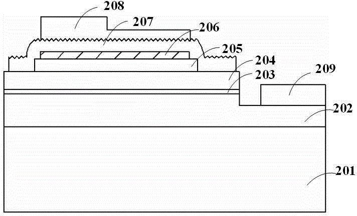
[0045] Such as Figure 12 As shown, another light-emitting diode device with a transparent conductive layer has the same general structure as the light-emitting diode device in Embodiment 1. The difference between the two mainly lies in: the first transparent conductive layer 206 and the current blocking layer of this embodiment The contact area of ​​205 is smaller than the upper surface area of ​​the current blocking layer 205; the upper surface of the first transparent conductive layer 206 has no roughness.

[0046] Such as Figure 7~12 As shown, another method for manufacturing a light-emitting diode device with a transparent conductive layer is roughly the same as that of the light-emitting diode device in Example 1, the difference mainly lies in: the first transparent conductive layer 206 and the second transparent conductive layer 207 The coating method is different. Specifically:

[0047] Such as Figure 7 As shown, a sapphire substrate 201 is provided; a firs...


PUM

PropertyMeasurementUnit
electrical conductoraaaaaaaaaa

Abstract

Provided are a light emitting diode (LED) having a transparent conductive layer, and manufacturing method thereof, the LED comprising: a substrate (101); a luminous epitaxial layer formed of semiconductor materials and formed on the substrate (101) by sequentially stacking from the bottom to the top a first limit layer (102), a luminous layer (103), and a second limit layer (104); a current barrier layer (105) formed on a local area of the luminous epitaxial layer; a transparent conductive structure (106, 107) formed on the current barrier layer (105) and extending to the surface of the luminous epitaxial layer, and divided into a light outlet region and a non-light outlet region, the non-light outlet region corresponding to the current barrier layer (105), and being thicker than the light outlet region, thus forming good ohmic contact between the transparent conductive structure (106, 107) and the luminous epitaxial layer, and reducing light absorption; and a P electrode formed on the non-light outlet region of the transparent conductive structure (106, 107). The transparent conductive structure (106, 107) ensures current scalability, lowers working voltage, and reduces light absorption.

Description

technical field [0001] The invention relates to a light-emitting diode and a manufacturing method thereof, more particularly to a light-emitting diode with a transparent conductive layer and a manufacturing method thereof. Background technique [0002] After years of development, light-emitting diodes (LEDs) have been widely used in different fields such as display, indication, backlight, and lighting. Group III-V compounds are currently the mainstream semiconductor materials for making light-emitting diodes, among which gallium nitride-based materials and aluminum gallium indium phosphide-based materials are the most common. The current spreading performance of traditional p-type III-V semiconductor materials is generally poor. In order to allow the current to be uniformly injected into the light-emitting layer, it is often necessary to add a transparent conductive layer on the p-type material layer. Among many materials that can be used as transparent conductive layers, s...

Claims


Application Information

Patent Timeline
Patent Type & Authority Patents(China)
IPC IPC(8): H01L33/38H01L33/00
CPCH01L33/38H01L2933/0016C23C14/086C23C14/24C23C14/5806C23C14/024C23C14/35H01L33/42C23C14/58H01L33/005H01L2933/0025H01L2933/0066
Inventor 尹灵峰林素慧郑建森洪灵愿刘传桂欧毅德陈功
Owner ANHUI SANAN OPTOELECTRONICS CO LTD
Why Eureka
Try Eureka