

A kind of preparation method of non-photosensitive polyimide passivation layer
A polyimide, non-photosensitive technology, which is applied in the production field of non-photosensitive polyimide passivation layers, can solve the problems of corrosion of top metal aluminum lines, poor morphology of non-photosensitive polyimide, etc.
- Summary
- Abstract
- Description
- Claims
- Application Information
AI Technical Summary
Problems solved by technology
Method used
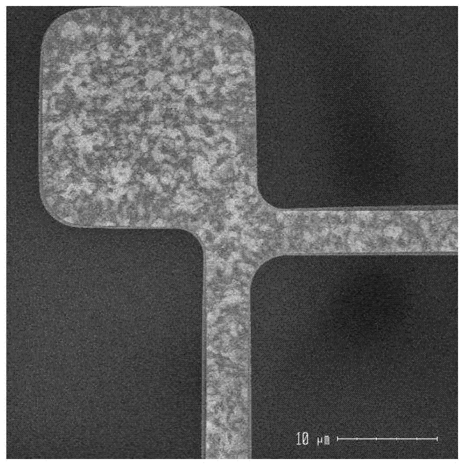
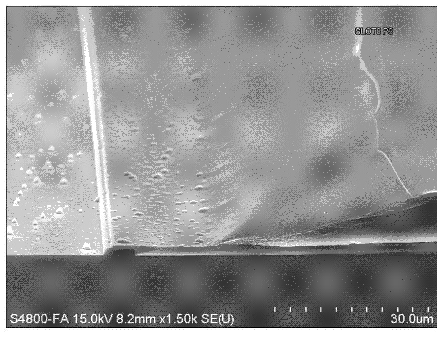
Image

Examples
Embodiment Construction
[0029] The present invention will be described in further detail below in conjunction with the accompanying drawings and embodiments.
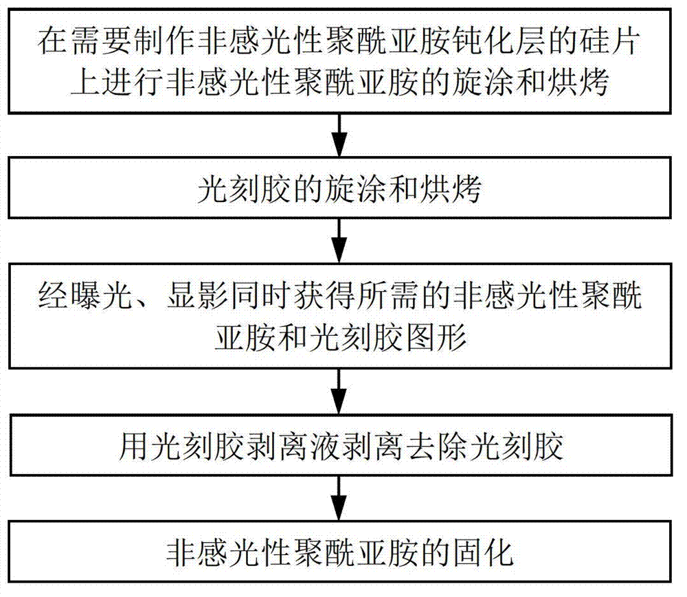
[0030] A kind of manufacture method of non-photosensitive polyimide passivation layer of the present invention, its technological process is as follows Figure 4 and Figure 5(A)-Figure 5(F) As shown, it specifically includes the following steps:
[0031] (1) As shown in Figure 5(A), spin-coat and bake non-photosensitive polyimide 400 on the silicon wafer 100 that needs to be made into a passivation layer: the top layer metal aluminum line on the silicon wafer 100 200 has been formed, or the pattern of the top layer aluminum metal line 200 and the dielectric film passivation layer 300 on the silicon wafer 100 has been formed, preferably, the top layer metal aluminum line 200 and the dielectric film passivation layer 300 on the silicon wafer 100 in this embodiment The pattern of the metallization layer 300 has been formed, and the formation p...
PUM
| Property | Measurement | Unit |
|---|---|---|
| wavelength | aaaaa | aaaaa |
| wavelength | aaaaa | aaaaa |
| wavelength | aaaaa | aaaaa |
Abstract
Description
Claims
Application Information