Method for forming structure with high depth-to-width ratio pattern

A technology with high aspect ratio and aspect ratio, which is applied in the field of forming structures with high aspect ratio patterns, and can solve problems such as edge burrs of implant barrier layer, over-etching of hard mask layer edge, affecting high-energy ion implantation and device characteristics, etc. , to achieve the effect of solving the shape problem and satisfying the device characteristics

Active Publication Date: 2019-02-12
SHANGHAI HUALI MICROELECTRONICS CORP
View PDF6 Cites 2 Cited by
  • Summary
  • Abstract
  • Description
  • Claims
  • Application Information

AI Technical Summary

Problems solved by technology

[0004] However, there are certain defects in the multilayer lithography technology. If the ratio of the thickness of the injection barrier layer to the critical dimension is too large, the injection barrier layer will be in the shape of a cone or a bowling ball; if the thickness of the injection barrier layer is too large, the hard mask layer is prone to edge over-etching, resulting in burrs at the edge of the implant barrier layer
All of the above defects will affect high-energy ion implantation and device characteristics

Method used


Image

  • Method for forming structure with high depth-to-width ratio pattern
  • Method for forming structure with high depth-to-width ratio pattern
  • Method for forming structure with high depth-to-width ratio pattern

Examples


Embodiment Construction

[0038] The technical solutions in the embodiments of the present invention will be clearly and completely described below in conjunction with the accompanying drawings in the embodiments of the present invention. Obviously, the described embodiments are only a part of the embodiments of the present invention, rather than all the embodiments. Based on the embodiments of the present invention, all other embodiments obtained by those of ordinary skill in the art without creative work shall fall within the protection scope of the present invention.

[0039] It should be noted that the embodiments of the present invention and the features in the embodiments can be combined with each other if there is no conflict.

[0040] The present invention will be further described below in conjunction with the accompanying drawings and specific embodiments, but it is not a limitation of the present invention.

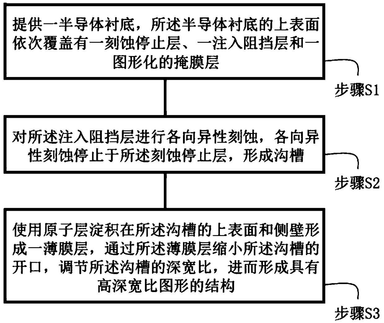
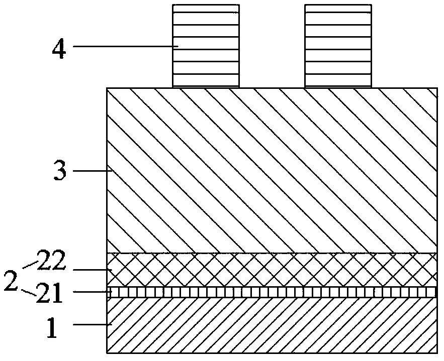
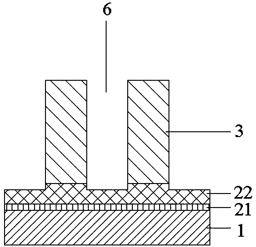
[0041] Such as figure 1 As shown, an exemplary embodiment of a method for forming a struct...


PUM


Abstract

The invention relates to a method for forming a structure with a high depth-to-width ratio pattern. The method includes the following steps: step S1. providing a semiconductor substrate, wherein an etching stop layer, an injection barrier layer and a patterned mask layer are covered on the upper surface of the semiconductor substrate in sequence; step S2. performing anisotropic etching on the injection barrier layer, stopping, by the anisotropic etching, at the etching stop layer to form a groove; step S3. forming a thin film layer on the upper surface and the side wall of the groove by usingatomic layer deposition, narrowing an opening of the groove through the thin film layer, adjusting the depth-to-width ratio of the groove, and then forming the structure with the high depth-to-width ratio pattern. The method has the advantages that as the thin film layer is formed on the upper surface and the side wall of the groove on the traditional thin film structure by using an ALD (atomic layer deposition) technology, and the opening of the groove is adjusted by adjusting the thickness of the thin film layer to form the high depth-to-width ratio pattern, the problems of small depth-to-width ratio of the traditional lithography process and the topography caused by the multi-layer lithography technology are solved.

Description

Technical field [0001] The present invention relates to the field of semiconductor manufacturing technology, and in particular to a method for forming a structure with a high aspect ratio pattern. Background technique [0002] In the Complementary Metal Oxide Semiconductor (CMOS) image sensor chip manufacturing process, high-energy ion implantation is performed on the structure of high aspect ratio graphics to achieve isolation between each pixel, thereby improving image clarity. To achieve high pixels per unit area. [0003] In some high-energy ion implantation processes, the line width is required to be 0.15 μm, the photoresist thickness is 0.4 μm, and the aspect ratio is greater than 20:1. If a traditional dielectric film structure is used, a high aspect ratio cannot be achieved through a traditional photolithography process (the aspect ratio is less than 5:1), and a small line width cannot be achieved. Therefore, in order to achieve a high aspect ratio, Tri-Layer technology i...

Claims


Application Information

Patent Timeline
IPC IPC(8): H01L21/3065H01L27/146
CPCH01L21/30655H01L27/1463H01L27/14687
Inventor 冯奇艳刘鹏唐在峰
Owner SHANGHAI HUALI MICROELECTRONICS CORP
Why Eureka
Try Eureka