
Method for manufacturing non-photosensitive polyimide passivation layer

一种聚酰亚胺、非感光性的技术,应用在非感光性聚酰亚胺钝化层的制作领域,能够解决非感光性聚酰亚胺形貌差、光刻胶残留、金属铝显影腐蚀等问题,达到解决非感光性聚酰亚胺形貌问题、防止光刻胶残留的效果

Active Publication Date: 2013-06-05
SHANGHAI HUAHONG GRACE SEMICON MFG CORP
View PDF3 Cites 12 Cited by
  • Summary
  • Abstract
  • Description
  • Claims
  • Application Information

AI Technical Summary

Problems solved by technology

[0004] The technical problem to be solved by the present invention is to provide a method for making a non-photosensitive polyimide passivation layer, so as to solve the problem of metal aluminum being corroded by development and non-photosensitive polyimide in the traditional non-photosensitive polyimide process. Poor morphology and photoresist residue

Method used


Image

  • Method for manufacturing non-photosensitive polyimide passivation layer
  • Method for manufacturing non-photosensitive polyimide passivation layer
  • Method for manufacturing non-photosensitive polyimide passivation layer

Examples


Embodiment Construction

[0032] The present invention will be described in further detail below in conjunction with the accompanying drawings and embodiments.

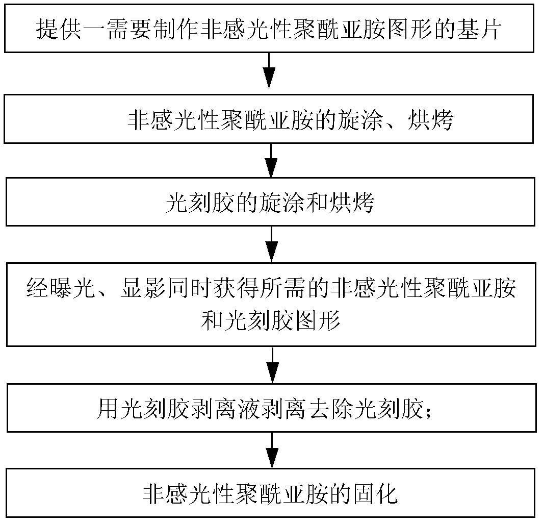
[0033] The invention discloses a method for making a non-photosensitive polyimide passivation layer, the process flow of which is as follows Figure 5 As shown in Figure 6, it specifically includes the following steps:

[0034] (1) As shown in Figure 6 (A), provide a substrate 1 that needs to make a non-photosensitive polyimide passivation layer, and the top layer metal wiring 2 and the dielectric layer passivation film 3 on this substrate 1 The pattern has been formed; the formation process generally adopts the conventional method in the field to form the top layer metal connection 2 on the substrate 1, then deposit the dielectric layer passivation film 3, and etch the dielectric layer passivation film at the position of the top layer metal connection 2 3. Form a contact hole; the dielectric layer passivation film 3 can be silicon nitride, s...


PUM


Abstract

The invention discloses a method for manufacturing a non-photosensitive polyimide passivation layer. Non-photosensitive polyimide is spin-coated and baked on a substrate on which a passivation layer is required to be manufactured, a layer of silica is grown by a low temperature method, photoresist is spin-coated and baked on the silica, exposure and developing are performed to obtain a photoresist pattern, the photoresist pattern is used as a mask layer, the silica is etched to form a pattern, the photoresist is stripped, pattern silica is used as a mask layer, the non-photosensitive polyimide is subjected to dry etching to form a pattern, the silica is removed by a drying back etching method, and finally, the curing is performed to obtain the non-photosensitive polyimide passivation layer. By means of the method for manufacturing the non-photosensitive polyimide passivation layer, problems that metallic aluminum is developed and corroded, morphology of the non-photosensitive polyimide is poor, photoresist residues exist and the like in terms of traditional non-photosensitive polyimide processes are solved.

Description

technical field [0001] The invention belongs to the manufacturing process of semiconductor integrated circuits, and relates to a method for manufacturing a passivation layer, in particular to a method for manufacturing a non-photosensitive polyimide passivation layer. Background technique [0002] Non-photosensitive polyimide (polyimide) materials have been widely used in the passivation layer process of semiconductor devices due to their good high temperature resistance, mechanical properties, electrical properties and chemical stability, in order to reduce various natural environments. And the damage caused by the working environment to the semiconductor device, thereby improving the reliability and stability of the device. [0003] The general traditional non-photosensitive polyimide passivation layer process is as follows: figure 1 As shown, firstly, the non-photosensitive polyimide is spin-coated and baked on the substrate that needs to make a non-photosensitive polyim...

Claims


Application Information

Patent Timeline
Patent Type & Authority Applications(China)
IPC IPC(8): H01L21/312
CPCH01L24/05H01L2224/05567H01L23/3192H01L21/02304H01L23/3171H01L21/76802H01L21/56H01L24/00H01L2224/05624H01L21/561H01L2924/00014H01L2924/12042H01L2224/05552H01L2924/00
Inventor 郭晓波
Owner SHANGHAI HUAHONG GRACE SEMICON MFG CORP
Learn More