Thin film solar cell with microcrystalline absorpber layer and passivation layer and method for manufacturing such a cell

A passivation layer and microcrystalline technology, applied in circuits, photovoltaic power generation, electrical components, etc., can solve problems such as good Voc and high crystallinity

Inactive Publication Date: 2013-04-10
OERLIKON SOLAR AG (TRUEBBACH)
View PDF2 Cites 4 Cited by
  • Summary
  • Abstract
  • Description
  • Claims
  • Application Information

AI Technical Summary

Problems solved by technology

However, with a defect passivation layer, using typical standard PECVD deposition parameters, it is possible to obtain high crystallinity (high Jsc) and good Voc

Method used


Image

  • Thin film solar cell with microcrystalline absorpber layer and passivation layer and method for manufacturing such a cell
  • Thin film solar cell with microcrystalline absorpber layer and passivation layer and method for manufacturing such a cell
  • Thin film solar cell with microcrystalline absorpber layer and passivation layer and method for manufacturing such a cell

Examples


Embodiment Construction

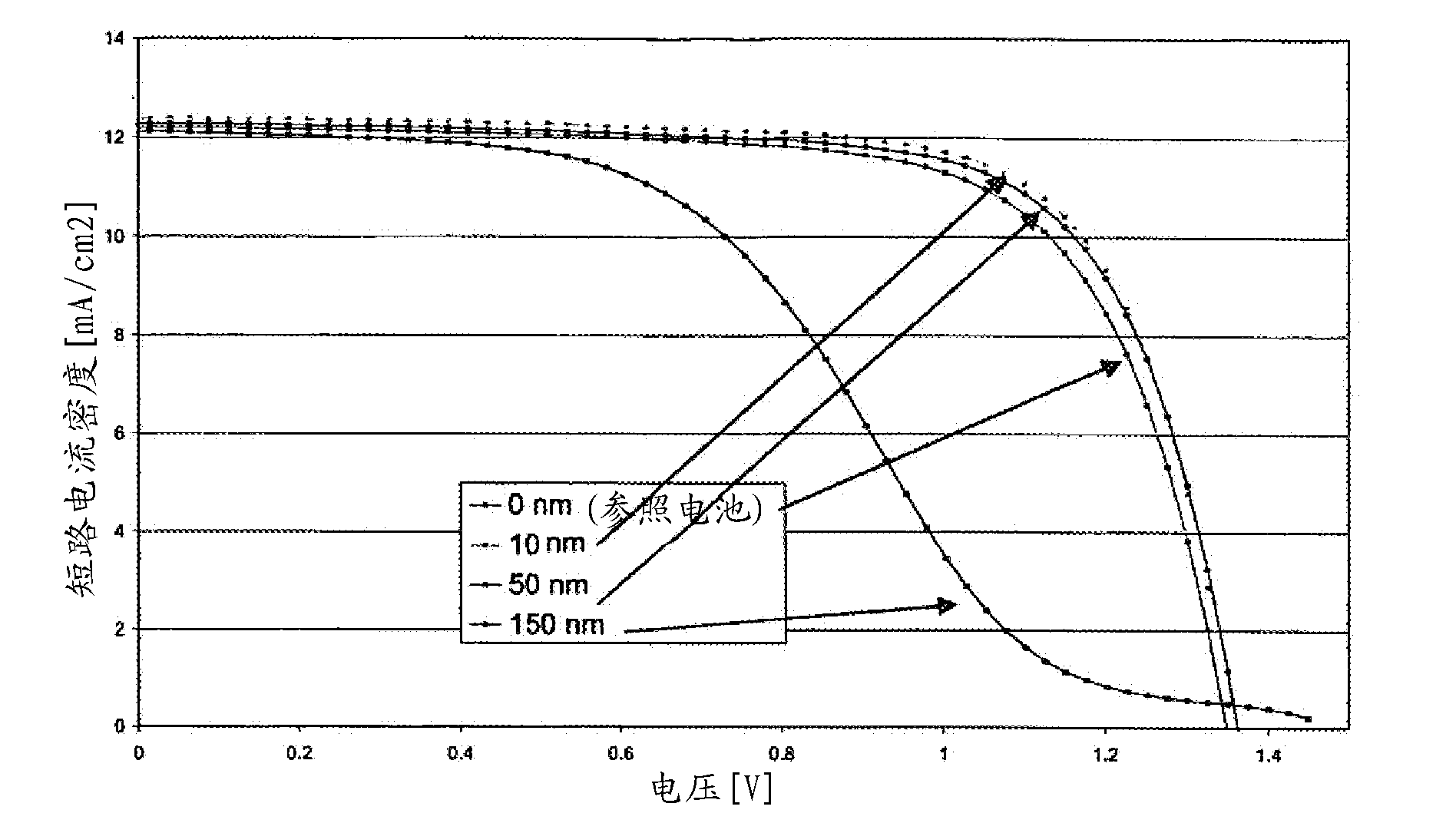
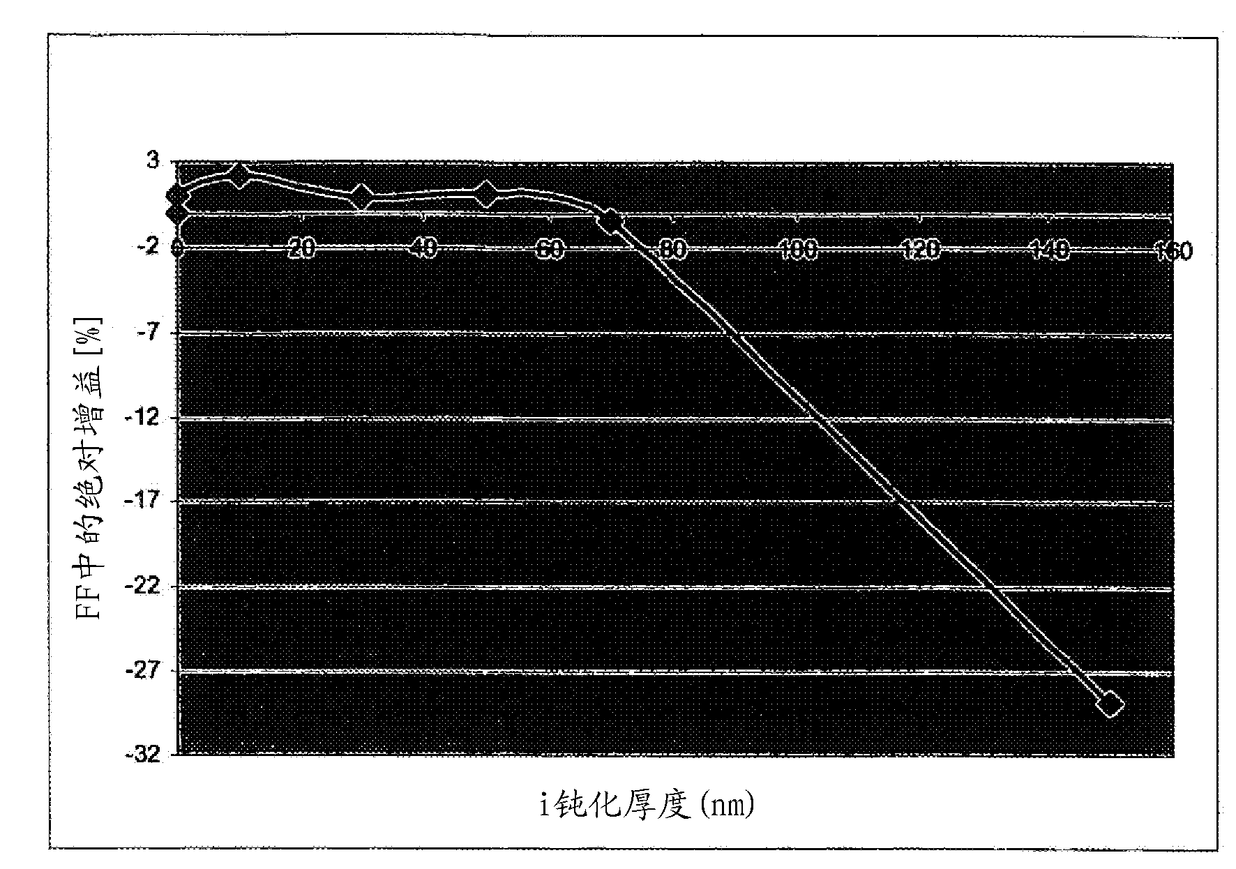
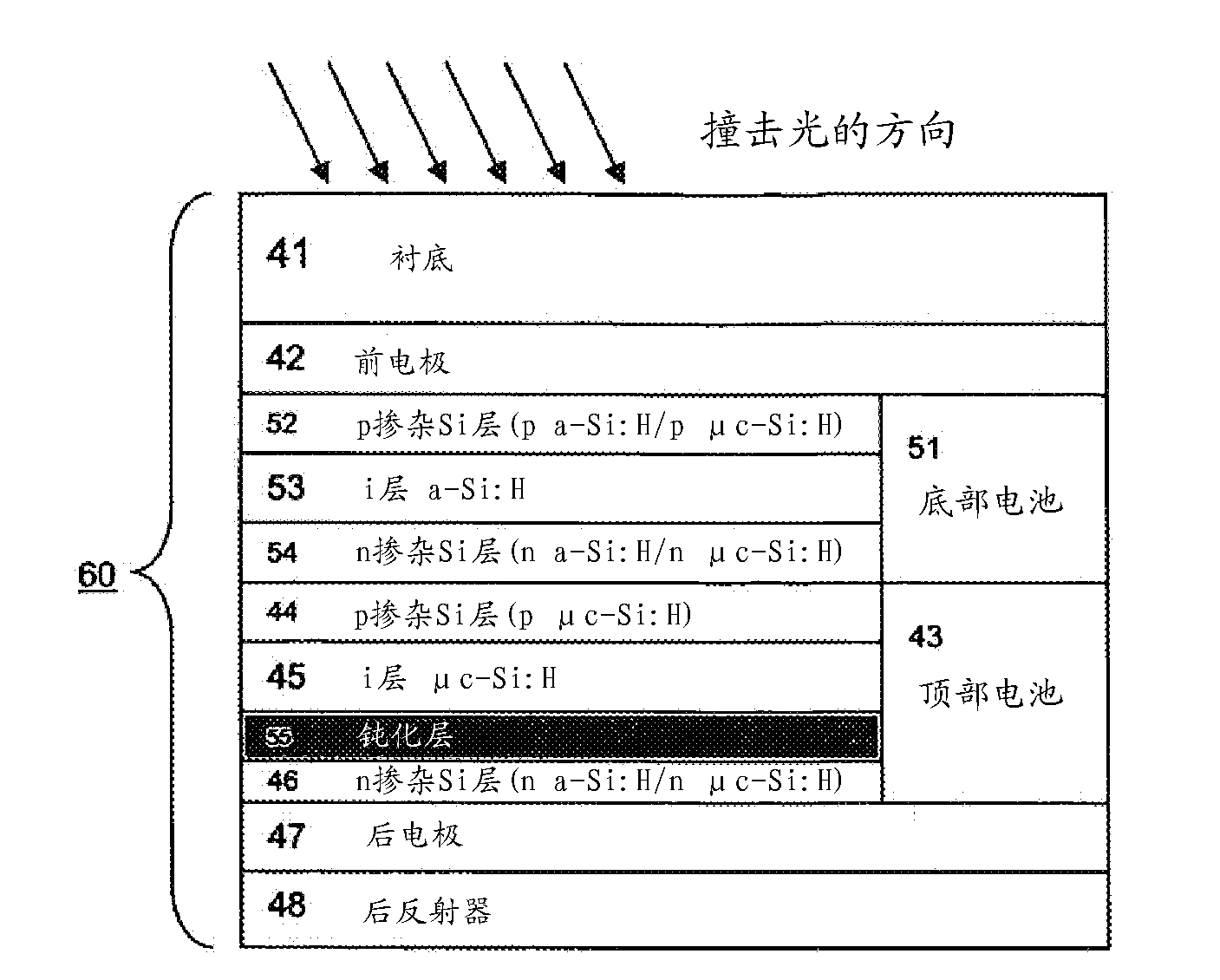
[0015] In the following illustrative examples, top-confined amorphous tandem cells were fabricated on native rough TCO (LPCVD-ZnO). A reference device 50 for comparison provides a top pin a-Si:H cell 51 with an i-layer 53 thickness of 250nm and 2000nm light with moderate crystallinity (50-55% bulk Raman crystallinity measured with a 780nm laser) The bottom μc-Si:H cell 43 of the active i-layer 45 . The passivation device 60 has the same i-layer thickness for the top and bottom cells, except that the deposition of the μc-Si:H i-layer 45 according to the invention is followed by the deposition of a fully amorphous i-layer 55 (passivation layer) of varying thickness. Passivated device 60 exhibits improved electrical performance (see FIG. 1 ). This suggests that the detrimental effects of certain defects in the underlying microcrystalline silicon layer are thus mitigated. In particular, recombination centers such as dangling bonds can be efficiently passivated with a-Si:H, and t...


PUM


Abstract

A Photovoltaic cell 60 includes a substrate 31, a front or first electrode 42 of transparent conductive oxide and at least one p-i-n junction 43 of microcrystalline silicon, said p-i-n junction 43 comprising a first n-doped silicon sub-layer 44 and a second p-doped silicon sub-layer 46 and a third sub-layer 45 with essentially intrinsic microcrystalline silicon. A passivation layer 45 comprising essentially intrinsic amorphous silicon is arranged a) between the microcrystalline intrinsic sub-layer 45 and n-doped silicon layer 46 or b) as a layer embedded in the microcrystalline intrinsic sublayer 45 or c) both. A method for manufacturing such a photovoltaic thin film silicon solar cell includes providing a transparent substrate 41 with a TCO front electrode 42 on it; depositing a p-doped Si layer 44, a microcrystalline silicon intrinsic layer 45, a passivation layer 55 from essentially intrinsic amorphous silicon, a n-doped Si layer 46 and a back electrode layer 48.

Description

[0001] The present invention relates to solar photovoltaic conversion devices, solar cells, and especially thin film silicon photovoltaic devices with improved performance due to the incorporation of passivation layer(s) within the photoactive crystallite portion of the device. field of invention [0002] Figure 4A shows a tandem junction silicon thin film solar cell known in the art. Such a thin film solar cell 50 generally includes a first or front electrode 42 stacked on a substrate 41, one or more semiconductor thin film p-i-n junctions (52-54, 51, 44-46, 43), and a second or rear electrode. Electrode 47. Each p-i-n junction 51, 43 or thin-film photoelectric conversion unit comprises an i-type layer 53, 45 sandwiched between a p-type layer 52, 44 and an n-type layer 54, 46 (p-type=positive doping, n-type=negative doping). The substantially intrinsic semiconductor layer i-type layer 53, 45 occupies most of the thickness of the thin-film p-i-n junction. In this context, s...

Claims


Application Information

Patent Timeline
Patent Type & Authority Applications(China)
IPC IPC(8): H01L31/075H01L31/076H01L31/0747H01L31/20
CPCH01L31/0747H01L31/075H01L31/076Y02E10/548H01L31/0216H01L31/042H01L31/20
Inventor J.赫策尔E.瓦拉特-绍瓦因S.贝纳格利L.卡斯滕斯X.穆尔通D.博雷洛
Owner OERLIKON SOLAR AG (TRUEBBACH)
Why Eureka
Try Eureka