Slow light waveguide device of photonic crystal based on two-dimensional silicon

A photonic crystal and optical waveguide technology, applied in the optical field, can solve the problems of inability to form slow light effects, destroying structural symmetry, weakening slow light effects, etc., achieving simple and easy efficiency, good signal fidelity, and large slow light bandwidth. Effect

Inactive Publication Date: 2013-04-17
QINGDAO UNIV
View PDF4 Cites 4 Cited by
  • Summary
  • Abstract
  • Description
  • Claims
  • Application Information

AI Technical Summary

Problems solved by technology

At present, there is no research on the application of two-dimensional gradient line defect waveguide structure to photonic crystal slow light; many researchers believe that the gradual change process destroys the symmetry of the structure, the slow light effect will be weakened, and even the slow light effect cannot be formed.
[0004] Existing technologies have proved that the slow light effect can be used in optical delay, all-optical buffering, optical storage, and light-material interaction. The photonic crystal structure has a small size and is easy to integrate. The slow light effect can be controlled by designing the structure. There are no special requirements for the working environment, and it can work at room temperature, which is convenient for coupling and matching with optical fiber systems. Moreover, the realization of photonic crystal slow-light structures will drive breakthroughs in all-optical buffering, all-optical information processing, and all-optical communication network applications. It will have a profound impact on the development of all-optical information; seek to design a two-dimensional silicon-based hole-shaped longitudinal gradient line-defect photonic crystal slow-light waveguide structure constructed by circular bow-shaped scattering elements, which can well achieve low dispersion and low group velocity Broadband slow light, widely used in the buffering and processing of all-optical information, has important practical application value

Method used


Image

  • Slow light waveguide device of photonic crystal based on two-dimensional silicon
  • Slow light waveguide device of photonic crystal based on two-dimensional silicon
  • Slow light waveguide device of photonic crystal based on two-dimensional silicon

Examples


Embodiment 1

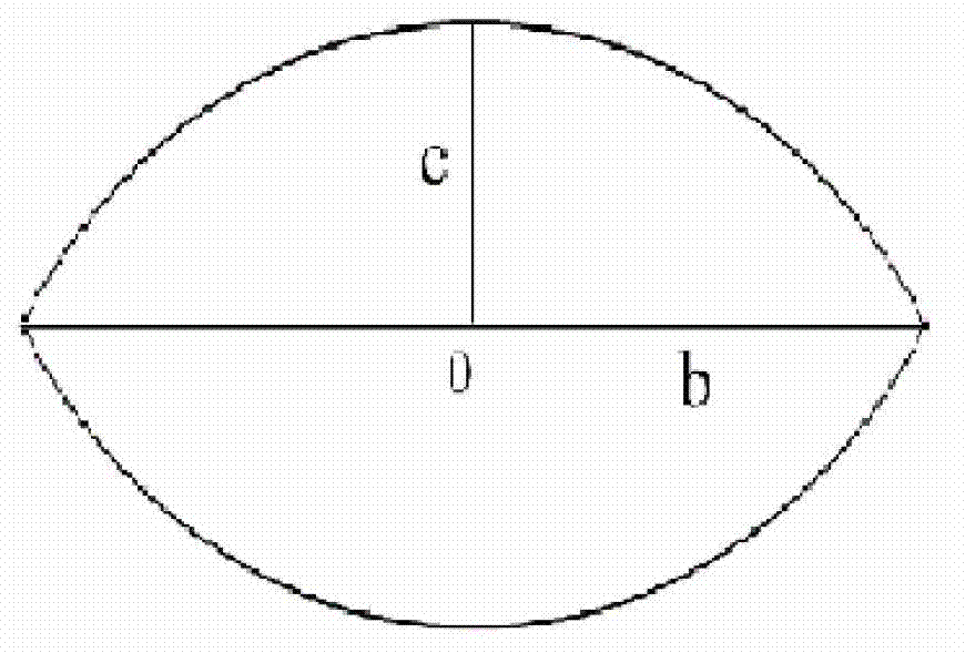
[0033] Example 1: Construct a low-scattering photonic crystal slow light waveguide device for the purpose of obtaining a larger bandwidth, using 1THz as the working frequency, a=65μm, the long axis b starts from 0.4a, and the gradual change step size △b=0.002a , take e=0.5 to obtain a terahertz frequency-domain two-dimensional silicon-based hole-shaped longitudinal gradient line-defect photonic crystal slow light waveguide device constructed by a specific circular segment scattering element, and use the above-mentioned implementation to obtain the group refractive index n of the device g =31.4, in low dispersion (group refractive index variation range n g within ±10%), ultra-low dispersion (group refractive index variation range n g Within ±1%) and close to zero dispersion, the bandwidths of slow light are 2.334 μm, 0.945 μm, and 0.91 μm respectively. The slow light waveguide device obtains a large flat bandwidth, and the slow light effect is stable.

Embodiment 2

[0034] Example 2: Construct a low-scattering photonic crystal slow light waveguide device for the purpose of obtaining a higher group refractive index. Other conditions are the same as in Example 1. Take e=0.35 to obtain a terahertz frequency constructed by another specific circular bow-shaped scattering element. Domain two-dimensional silicon-based hole-shaped longitudinal gradient line defect photonic crystal slow light waveguide structure, using the above implementation scheme, the group refractive index n of the device is obtained g =95.0, in the three cases of low dispersion, ultra-low dispersion and near-zero dispersion, the bandwidths of slow light are 0.736 μm, 0.438 μm, and 0.20 μm, indicating that this kind of slow light waveguide device can not only obtain a lower group velocity, but also A large flat bandwidth can be obtained, and the slow light effect is very stable. In the case of ensuring low dispersion, the group velocity and the slow light bandwidth can be flex...


PUM

PropertyMeasurementUnit
lattice constantaaaaaaaaaa
refractive indexaaaaaaaaaa

Abstract

The invention belongs to the technical field of the optics and relates to a slow light waveguide device of a photonic crystal based on two-dimensional silicon. The slow light waveguide device is characterized in that 6-10 rows of circular-segment scatterers with the center line of a two-dimensional silicon slice as the symmetrical axis are dug on the surface of the two-dimensional silicon slice in the direction of the long side of the two-dimensional silicon slice in sequential arrangement mode, and a row not dug with the circular-segment scatterers is reserved on the symmetrical axis of the two-dimensional silicon slice to form a line defect; 5-30 circular-segment scatterers are dug on each of the 6-10 rows at equal interval; each circular-segment scatterer is formed by two semi-circle segments, and hollowed through circular-segment scatterers sequentially arranged on the two-dimensional silicon slice are of symmetrical structures; the direction of the line defect is parallel to the long axis direction of the circular-segment scatterers; and the arrangement structure of the circular-segment scatterers is fixed. The slow light waveguide device does not need a complex and large system, has the advantages of being small in volume, low in cost, high in stability and efficiency, simple and practicable, is high in group refractivity, large in slow light bandwidth and good in signal fidelity and is a novel photonic crystal slow light structure.

Description

Technical field: [0001] The invention belongs to the field of optical technology, and relates to a two-dimensional silicon-based photonic crystal slow light waveguide device, in particular to a gradual line defect photonic crystal slow light waveguide structure, which is a two-dimensional terahertz frequency domain constructed by circular bow-shaped scattering elements. Silicon-based porous longitudinal gradient line defect photonic crystal slow light waveguide structure. Background technique: [0002] The slow light effect is that the group velocity of electromagnetic waves is much lower than the speed of light, so as to facilitate the buffering and processing of transmitted information, and can be widely used in fields such as optical delay lines and buffers. The photonic crystal slow light structure or device has incomparable advantages in the application of all-optical communication systems and all-optical information processing due to its small and compact structure, lo...

Claims


Application Information

Patent Timeline
Patent Type & Authority Applications(China)
IPC IPC(8): G02F1/365G02F1/355G02B6/122
Inventor 万勇潘淑娣郭月
Owner QINGDAO UNIV
Why Eureka
Try Eureka