
Package Substrate Structure

A technology for packaging substrates and structures, applied in electrical components, electrical solid devices, circuits, etc., can solve the problems of passive component design flexibility and low reusability, and achieve the effect of reducing test costs

Active Publication Date: 2016-12-28
SUZHOU ASEN SEMICON CO LTD
View PDF8 Cites 0 Cited by
  • Summary
  • Abstract
  • Description
  • Claims
  • Application Information

AI Technical Summary

Problems solved by technology

[0006] In view of this, the present invention provides a packaging substrate structure to solve the problem of low design flexibility and low reusability of passive components in the packaging substrate structure existing in the prior art

Method used


Image

  • Package Substrate Structure
  • Package Substrate Structure
  • Package Substrate Structure

Examples


Embodiment Construction

[0017] The following descriptions of the various embodiments refer to the accompanying drawings to illustrate specific embodiments in which the present invention can be practiced. Furthermore, the directional terms mentioned in the present invention are, for example, up, down, top, bottom, front, back, left, right, inside, outside, side, surrounding, central, horizontal, transverse, vertical, longitudinal, axial, The radial direction, the uppermost layer or the lowermost layer, etc. are only directions referring to the attached drawings. Therefore, the directional terms used are used to illustrate and understand the present invention, but not to limit the present invention.

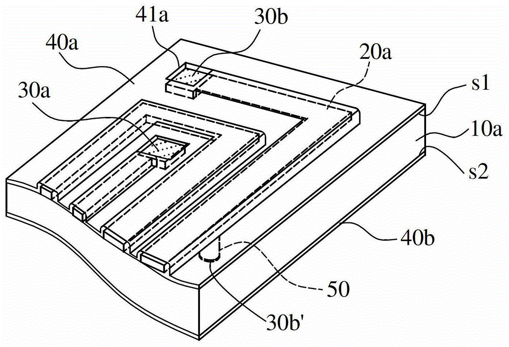
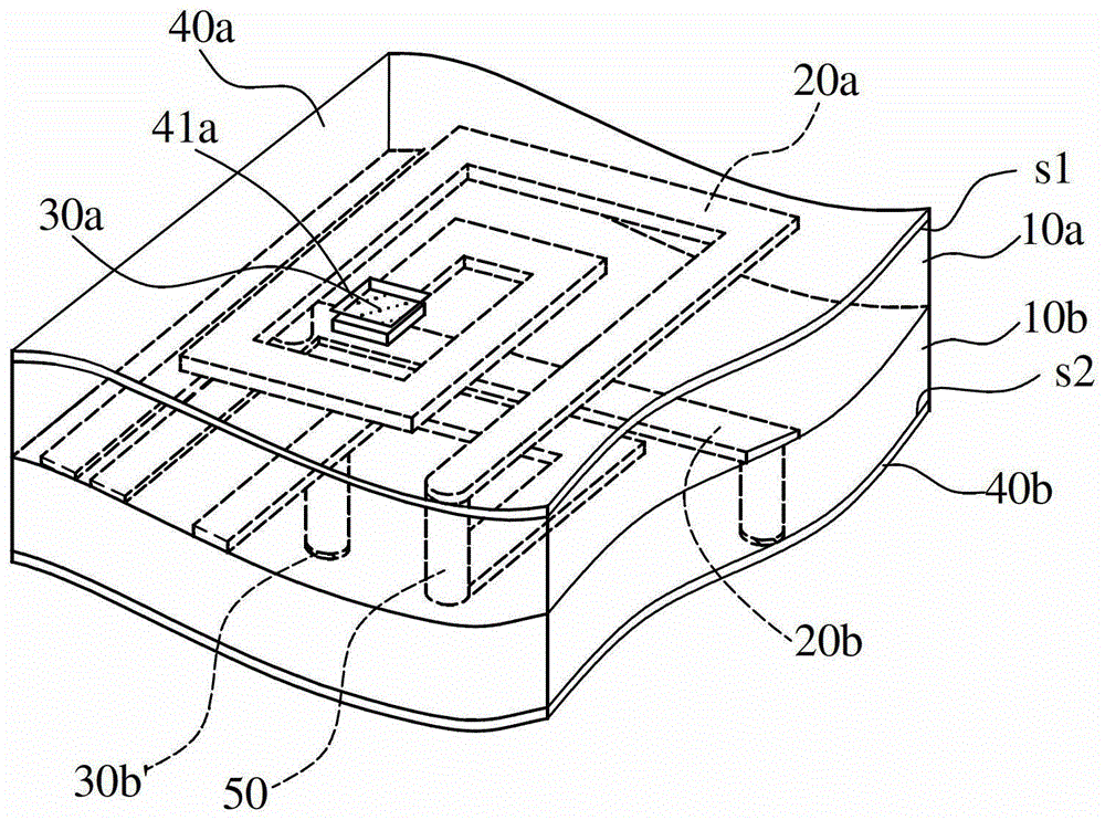
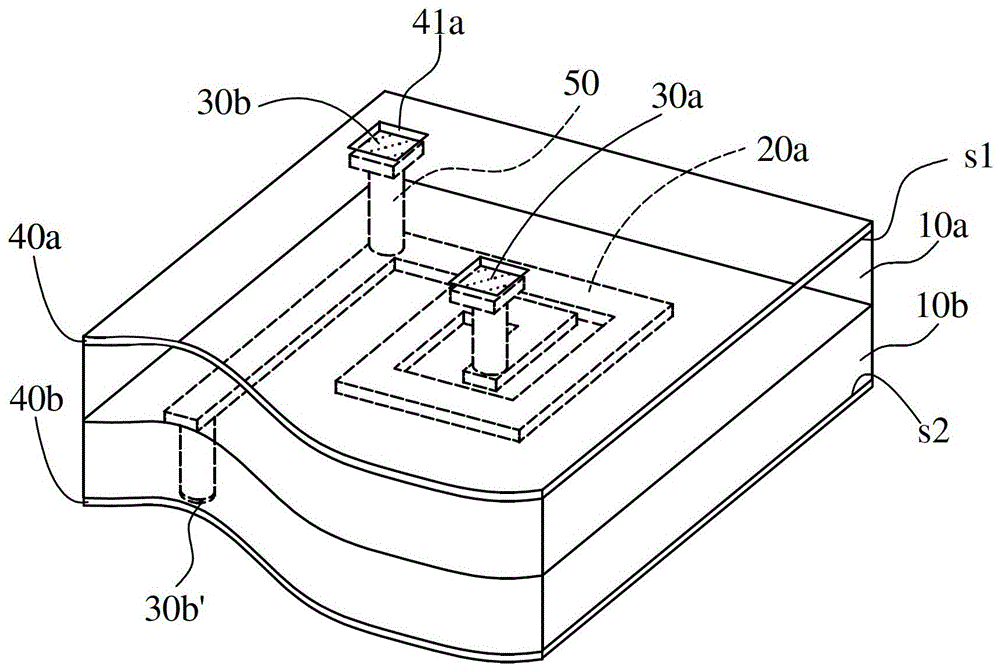
[0018] Please refer to figure 1 As shown, the packaging substrate structure of an embodiment of the present invention has an upper surface and a lower surface, and mainly includes: at least one dielectric layer 10a, an inductor body 20a, at least one first connection pad 30a and at least two second conne...


PUM


Abstract

The invention discloses a package substrate structure, which has an upper surface and a lower surface, and is characterized by comprising an inductor body arranged between the upper surface and the lower surface, at least one dielectric layer arranged between the upper surface and the lower surface, at least one first connecting pad exposed on the upper surface and electrically connected to one position of the inductor body, and at least two second connecting pads exposed on the upper surface or the lower surface and electrically connected with at least other two different positions of the inductor body.

Description

technical field [0001] The present invention relates to a structure of a packaging substrate, in particular to a structure of a packaging substrate with multiple connection locations for selection to adjust the inductance value. Background technique [0002] In the known electronic assembly technology, various electronic components, such as passive elements (passive elements), are adhered to substrates or printed circuit boards by using surface mount technology (SMT). Since the electronic components are exposed on the surface of the substrate, this causes many problems, such as occupying the bonding surface area of ​​the substrate. In addition, the surface-bonded passive components are electrically transmitted to the substrate by using solder paste, guide pins, bonding wires, etc. If the length of the sexual path is too long, it is easy to interfere with the high-frequency line and cause parasitic effects. [0003] Furthermore, the combination of various surface-bonded pass...

Claims


Application Information

Patent Timeline
Patent Type & Authority Patents(China)
IPC IPC(8): H01L23/64H01L23/498
CPCH01L2224/48091
Inventor 郭桂冠
Owner SUZHOU ASEN SEMICON CO LTD
Learn More