System and method for timing calibration of time-interleaved data converters

a technology of time-interleaved data and system, applied in the field of system and method for timing calibration of time-interleaved data converter, can solve the problems of significant memory requirements affecting the physical size and cost of manufacturing a data conversion system, the inability of systems to analyze incoming analog waveforms in the same way as offset and gain mismatches, and the inability to accurately calculate the timing error, etc., to achieve the effect of reducing test cost, reducing software suppor

Active Publication Date: 2006-12-12
KEYSIGHT TECH
View PDF3 Cites 56 Cited by
  • Summary
  • Abstract
  • Description
  • Claims
  • Application Information

AI Technical Summary

Benefits of technology

[0016]Other embodiments of the invention comprise methods in which coherent averaging of a periodic waveform is used to estimate the relative time delay of data converter sampling slices. This method requires minimal hardware modifications to the present converter architecture. A separate calibration controller uses these relative time delay estimates to iteratively adjust the clocking of each sampling slice. On-chip calibration for a complex interleaved data converter such as, for example, Agilent Technologies Inc.'s 20 GSa / s ADC, reduces the software support it requires. Built-in calibration according to embodiments of the present invention have the added advantage of reduced test time thereby reducing test cost and reduced calibration time in the end application.
[0017]Certain embodiments of the invention apply a calibration signal to a data converter to be calibrated. The calibration signal frequency has a defined ratio to the sample clock frequency on the converter to be calibrated; it is phase locked to a sample clock signal. In some embodiments, the calibration signal is not required to be perfectly locked to the converter's sample clock (see cycle slip). Using a calibration frequency that is related to the sample clock signal in certain embodiments minimizes the amount of sample storage required to calibrate the data converter.
[0018]Other embodiments of the present invention can be used to calibrate converters on separate instruments. Applications which require that the instruments be interleaved or time-synchronized can be performed more accurately following the calibration of the data converters according to certain embodiments of the present invention.

Problems solved by technology

The capacity or bandwidth of systems analyzing incoming analog waveforms is limited by the sampling rates of component ADCs.
While interleaving components such as ADCs or DACs is a powerful technique for increasing the maximum sampling rate of a signal processing system, the performance of interleaved converters is limited by offset and gain mismatches as well as by timing errors between interleaved slices.
Significant memory requirements impact the physical size and cost of manufacturing a data conversion system.
Unfortunately, long capture records demand more high speed sample storage, such as high speed RAM, and sample storage is limited in high-speed ADCs.
Off-chip methods for timing calibration that use memory external to a data converter tend to be more computationally complex and necessarily much slower.
A direct implementation of these off-chip methods for on-chip calibration is inefficient and computationally intensive.
Lastly, although few data converters have on-chip timing calibration systems, some already incorporate timing adjustment circuits.
A remaining hurdle in implementing on-chip timing calibration is determining those timing adjustments to be made by the timing adjustment circuits.

Method used


Image

  • System and method for timing calibration of time-interleaved data converters
  • System and method for timing calibration of time-interleaved data converters
  • System and method for timing calibration of time-interleaved data converters

Examples


examples

[0042]The following examples are included to demonstrate preferred embodiments of the invention. It should be appreciated by those of skill in the art that the techniques disclosed in the examples which follow represent techniques discovered by the inventor to function well in the practice of the invention, and thus can be considered to constitute preferred modes for its practice. However, those of skill in the art should, in light of the present disclosure, appreciate that many changes can be made in the specific embodiments which are disclosed and still obtain a like or similar result without departing from the spirit and scope of the invention. While the following examples refer to specific devices, other devices such as, for example, DACs and other data converters are used in other embodiments of the present invention that incorporate the exemplary material.

I. General Application

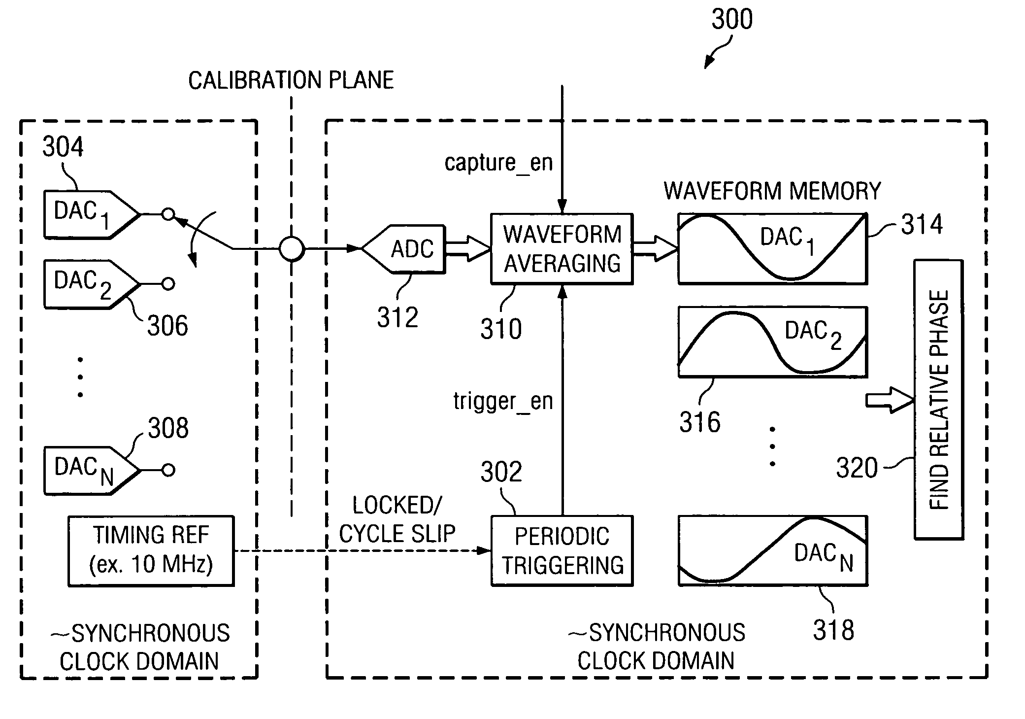
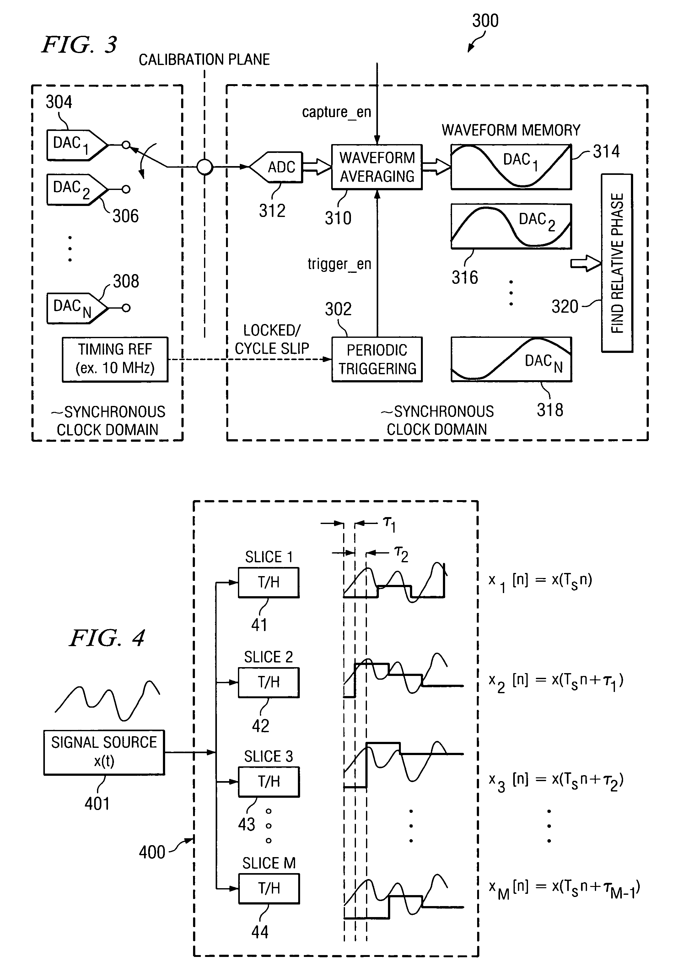
[0043]FIG. 4 illustrates the operation of an interleaved ADC 400. Timing calibration proceeds by appl...


PUM


Abstract

A method for calibrating time interleaved samplers comprising applying a calibration signal to a time-interleaved sampling device, wherein the signal is coherent with at least one sample clock on the device and is periodic and has a predetermined spectral content and frequency, sampling, by said time-interleaved sampling device, the calibration signal at a plurality of phases to form samples, averaging the formed samples, and calculating the phase error of each sample based on the average calibration signal sample.

Description

BACKGROUND OF THE INVENTION[0001]All digital systems that interact with the real world must convert continuous analog signals into a discrete representation and / or convert those discrete representations back into continuous signals. Devices that bridge the gap between the analog and digital world are known as data converters. Not surprisingly, digital-to-analog converters (DACs) and analog-to-digital converters (ADCs) are employed in a wide variety of applications including telecommuncations, medical imaging, consumer electronics, and general purpose measurement. Systems comprising DAC and ADC components can be characterized by their sampling rate, which is a measurement of how frequently the system converts an analog voltage to a digital sample or a digital sample to an analog voltage. The capacity or bandwidth of systems analyzing incoming analog waveforms is limited by the sampling rates of component ADCs.[0002]A current approach to increase the overall sampling rate of a data co...

Claims


Application Information

Patent Timeline
Patent Type & Authority Patents(United States)
IPC IPC(8): H03M1/10
CPCH03M1/10H03M1/1205H03M1/662
Inventor FERNANDEZ, ANDREW D.SRIKANTAM, VAMSI K.NEFF, ROBERT M. R.POULTON, KENNETH D.
Owner KEYSIGHT TECH
Why Eureka
Try Eureka