Inter-dice signal transfer methods for integrated circuits

a signal transfer and integrated circuit technology, applied in the direction of basic electric elements, semiconductor/solid-state device testing/measurement, instruments, etc., can solve problems such as electrical shorts, achieve the effects of reducing testing costs, simplifying connections, and providing flexibility to avoid defective circuits

Inactive Publication Date: 2007-01-09
ALPHA & OMEGA SEMICON LTD
View PDF3 Cites 54 Cited by
  • Summary
  • Abstract
  • Description
  • Claims
  • Application Information

AI Technical Summary

Benefits of technology

[0008]The primary objective of the present invention is to provide an effective data transfer method to support parallel operations in a large number of IC dice. One objective of this invention is to simplify the connections to support wafer level tests. The other objective is to test a large number of dice in parallel to reduce testing cost. Another important objective of the present invention is to provide the flexibility to avoid defective circuits. Yet another objective is to provide wafer level connections without using additional fabrication processes. The other primary objective of this invention is to build multiple dice integrated circuits to achieve unprecedented performance. These and other objectives of the present invention are achieved by inter-dice data transfer methods of the present invention. Each individual die of the present invention contains internal circuits to control data transfer to nearby dice. Wafer level data transfer is achieved by a series of inter-dice data transfers. The distance between the drivers and the receivers of inter-dice data transfer circuits of the present invention is very short. It is therefore possible to use a small number of small area wafer level conductive lines to support wafer level parallel processing activities. The metal lines in the scribing lane can be short and narrow. They are unlikely to cause electrical shorts during scribing process. External connections are provides by short conductive lines at the peripherals of a wafer. It is often possible to use a small number of external signals to control parallel processing for thousands of dice. The control logic in each die also can be programmed to avoid defective circuits in the wafer. It is therefore possible to build an IC containing many dice with excellent yields.

Problems solved by technology

They are unlikely to cause electrical shorts during scribing process.

Method used


Image

  • Inter-dice signal transfer methods for integrated circuits
  • Inter-dice signal transfer methods for integrated circuits
  • Inter-dice signal transfer methods for integrated circuits

Examples


Embodiment Construction

[0041]The present invention can be used for extremely powerful and complex applications. To demonstrate these complex applications, we start with simpler examples familiar to the current art. More and more complex examples are introduced until the full capability of the present invention is demonstrated. It should be understood that these particular examples are for demonstration only and are not intended as a limitation on the present invention.

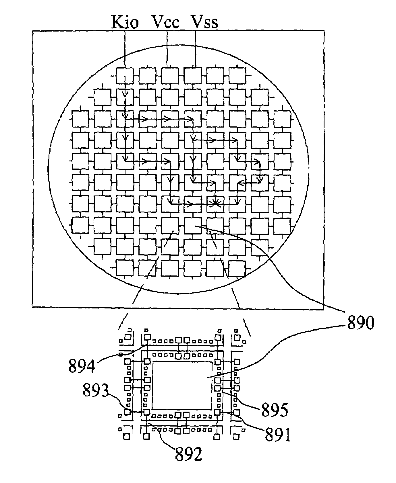
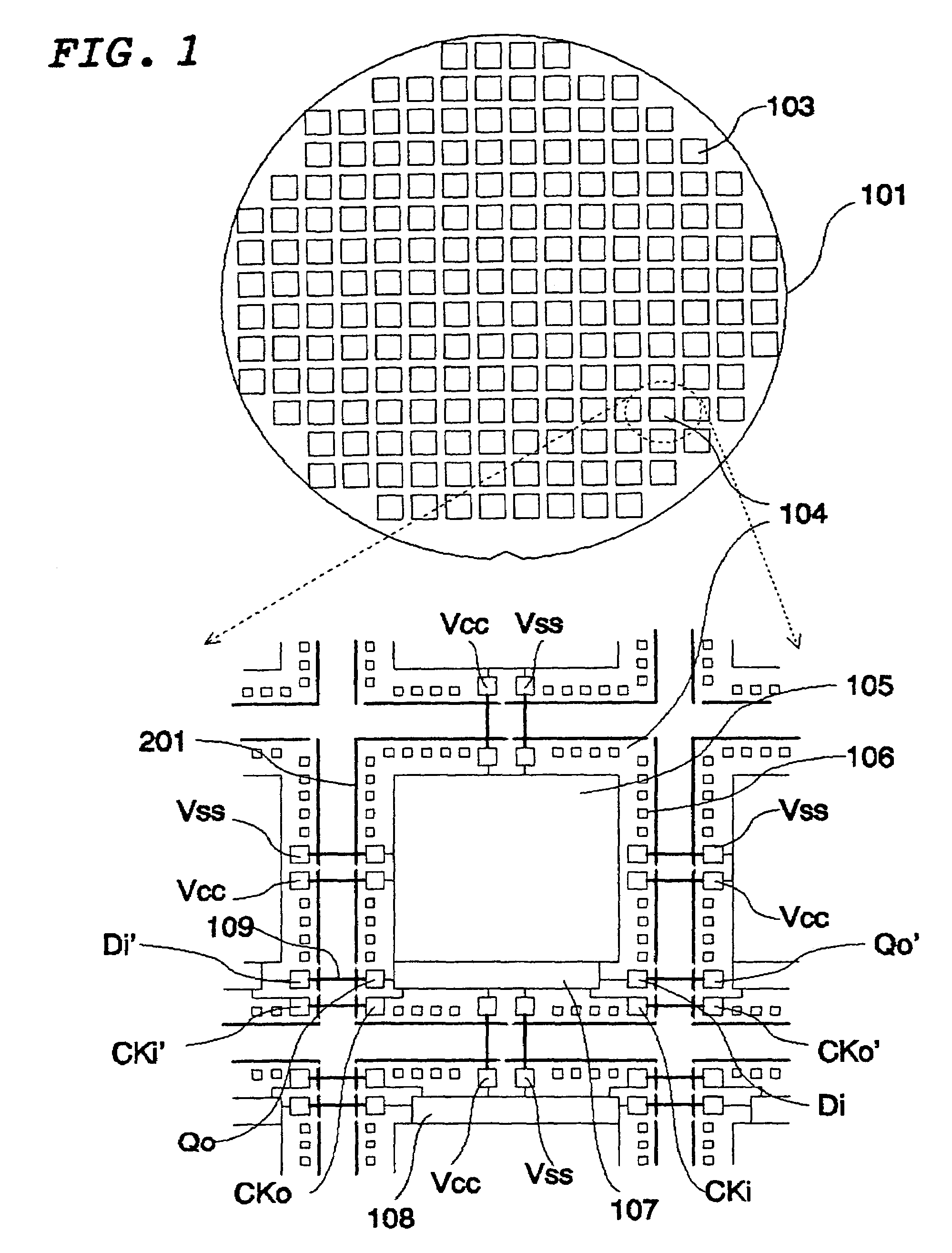
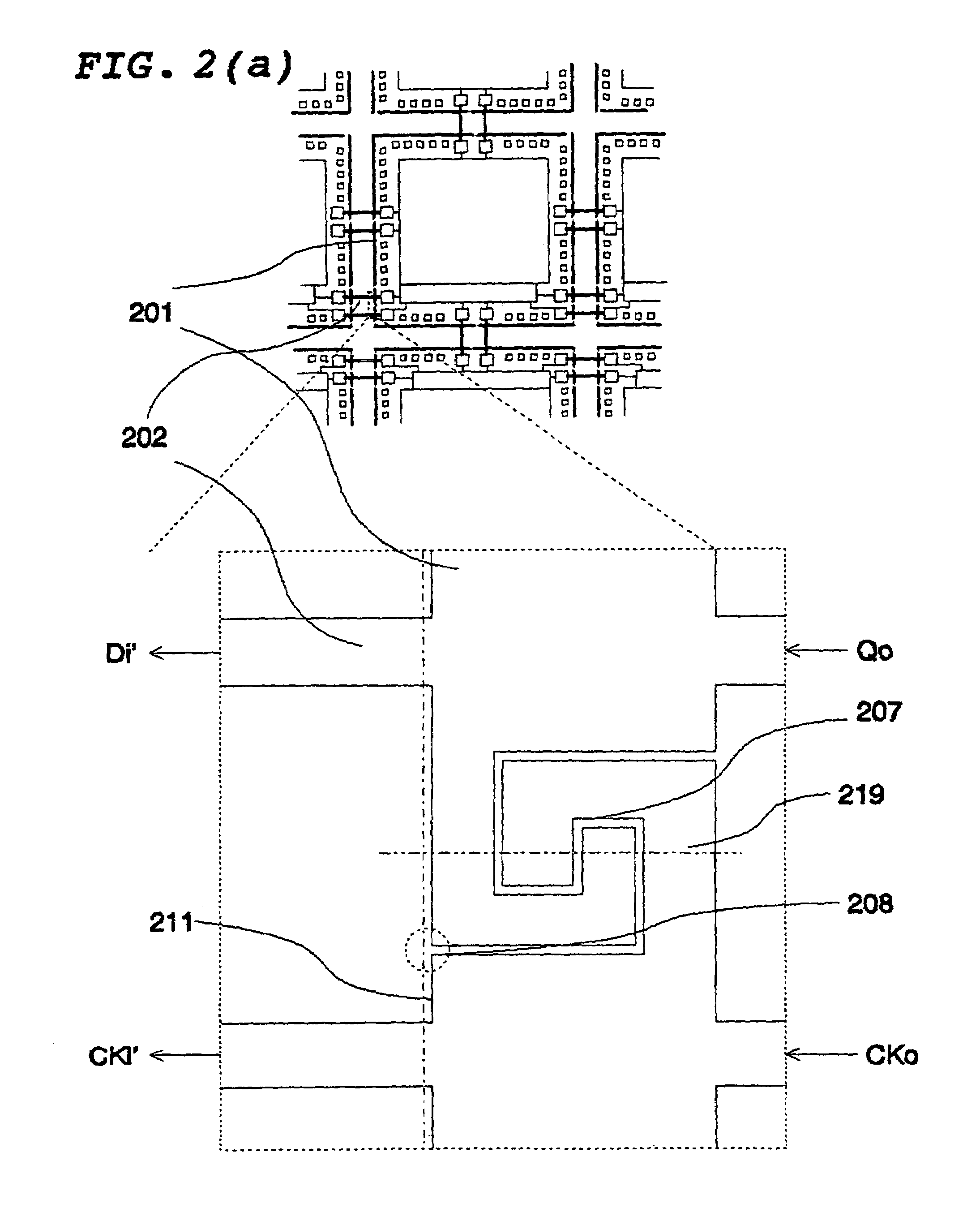
[0042]FIG. 1 illustrates the wafer-level connections in a semiconductor wafer (101) of the present invention. This wafer (101) contains a plurality of integrated circuit dice (103, 104) that are represented by rectangles. One of the circuit die (104) is magnified to reveal more details as shown in the lower diagram of FIG. 1. Each die contains core circuits (105), testing circuitry (107), and a plurality of bonding pads (106). The core circuits (105) support desired applications of the IC. The testing circuitry (107) executes tests to make s...


PUM


Abstract

The present invention discloses novel methods to transfer data between a plurality of integrated circuit dice on a semiconductor wafer. Each individual die contains internal circuits to control data transfer to nearby dice. Wafer level data transfer is achieved by a series of inter-dice data transfers. It is therefore possible to use a small number of small area metal lines to support wafer level parallel processing activities. External connections are provided by a small number of bonding pads on each wafer. The load on each external bounding pad is by far lower than that of prior art wafer level connections. These inter-dice data transfer mechanism also can be programmed to avoid defective circuitry. This invention has been used to support wafer level functional tests and wafer level burn-in tests. A Testing system of the present invention can test thousands of dice in parallel using simple testing equipment. Testing costs for integrated circuits are therefore reduced dramatically. The present application also makes it possible to build large area IC containing multiple dice. Extremely powerful products are realized using parallel processing capability of such multiple die integrated circuits.

Description

[0001]This is a Continuation in part Application of a previously filed Application with Ser. No. 10 / 115,836 filed on Apr. 2, 2002, now abandoned. Application Ser. No. 10 / 115,836 is a Divisional Patent Application of another application Ser. No. 08 / 941,786 filed on Sep. 30, 1997 by the Applicant of this invention now issued into U.S. Pat. No. 6,427,222 on Jul. 30, 2003.FIELD OF THE INVENTION[0002]The present invention relates to signal transfer methods to support parallel processing in a large number of integrated circuits, and particularly to methods to design multiple dice integrated circuits.BACKGROUND OF THE INVENTION[0003]Current art integrated circuit (IC) fabrication techniques involve formation of a plurality of individual IC devices on a single semiconductor substrate, termed a “wafer”. After fabrication is completed, the wafer is scribed to separate the individual IC devices called “dice”. Usually the individual dice are spaced apart from one another on the wafer to accommo...

Claims


Application Information

Patent Timeline
Patent Type & Authority Patents(United States)
IPC IPC(8): H01L23/58H01L29/40G01R31/28G01R31/3185
CPCG01R31/2856G01R31/318505G01R31/318511H01L22/32G01R31/2831G01R31/2884H01L2224/0603H01L2924/3011H01L2924/0002H01L2223/5448H01L2224/05554H01L2924/00
Inventor SHAU, JENG-JYE
Owner ALPHA & OMEGA SEMICON LTD
Why Eureka
Try Eureka