Full-automatic wafer test method and equipment accomplishing the method

A wafer test, fully automatic technology, applied in the direction of semiconductor/solid-state device test/measurement, electronic circuit test, single semiconductor device test, etc., can solve problems such as inability to judge the accuracy of dots, increase wafer test time, etc., to achieve test Low cost, high degree of automation and high efficiency

Inactive Publication Date: 2008-09-10
无锡市易控系统工程有限公司
View PDF0 Cites 55 Cited by
  • Summary
  • Abstract
  • Description
  • Claims
  • Application Information

AI Technical Summary

Problems solved by technology

This manual operation greatly increases the wafer test time, and when changing different types of chips for testing, the new probes must be manually adjusted, and then manually set the parameters
The accuracy of the test process can not be judged

Method used


Image

  • Full-automatic wafer test method and equipment accomplishing the method
  • Full-automatic wafer test method and equipment accomplishing the method
  • Full-automatic wafer test method and equipment accomplishing the method

Examples


Embodiment Construction

[0048] The present invention will be further described below in conjunction with specific drawings and embodiments.

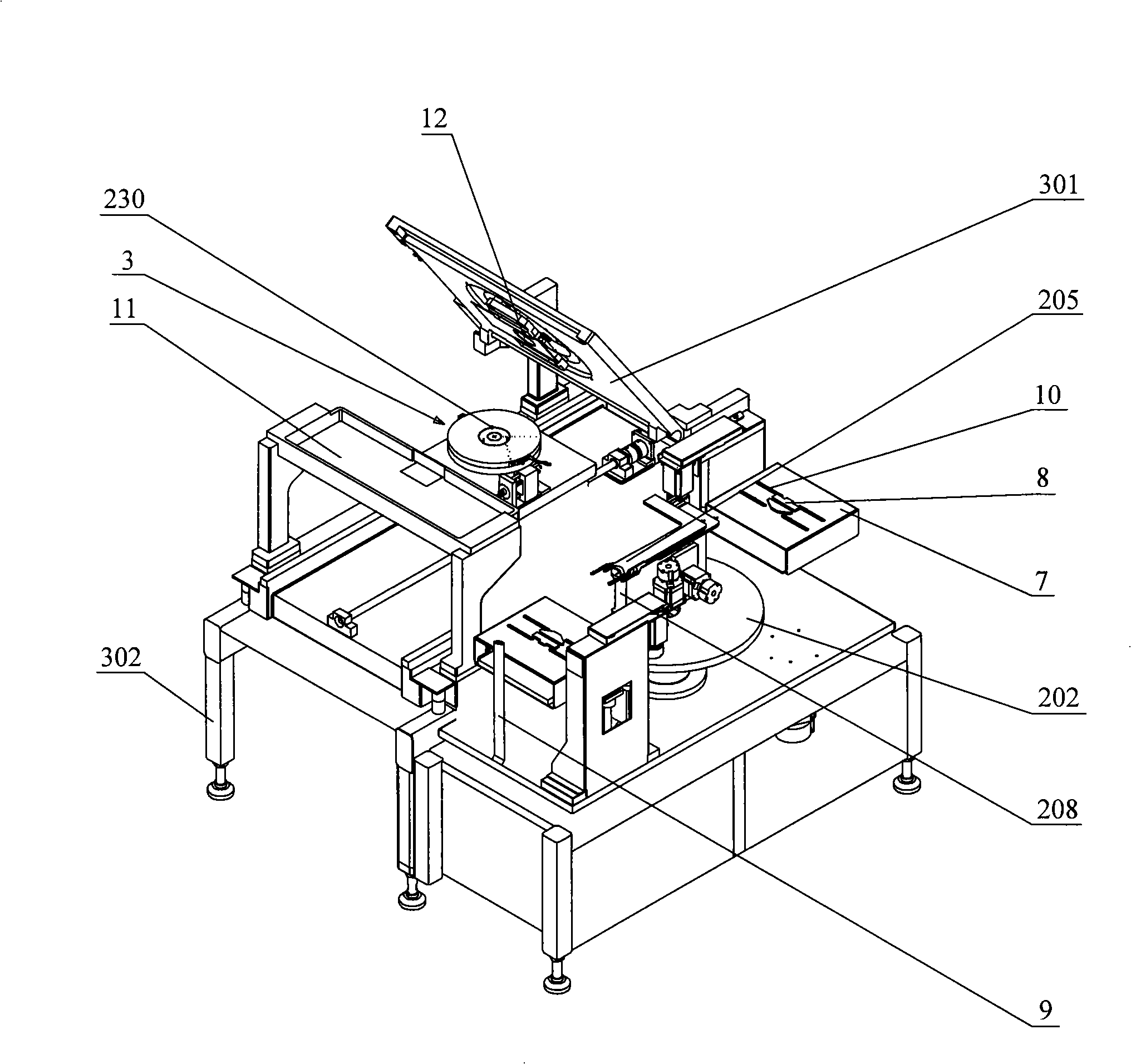
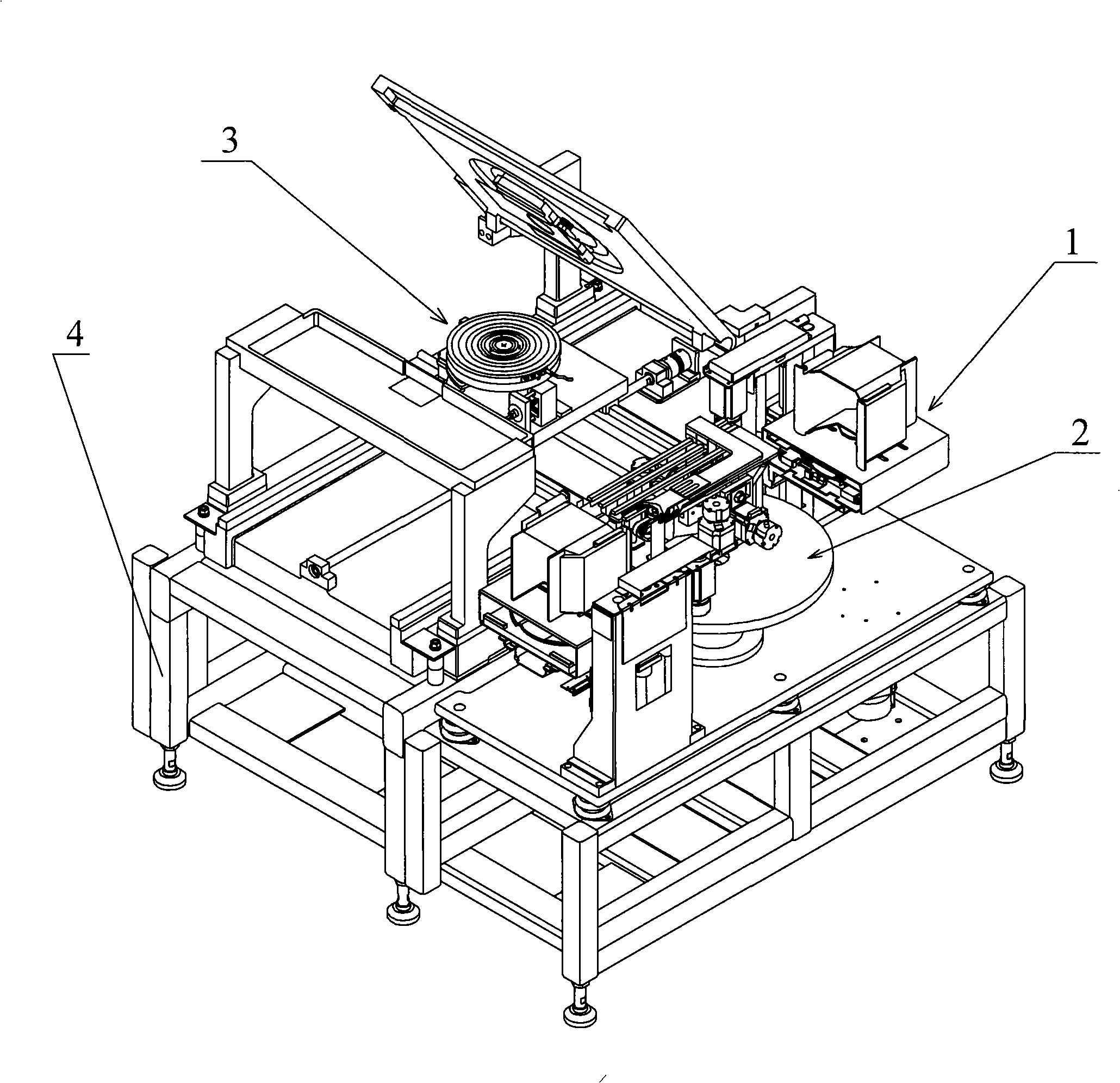
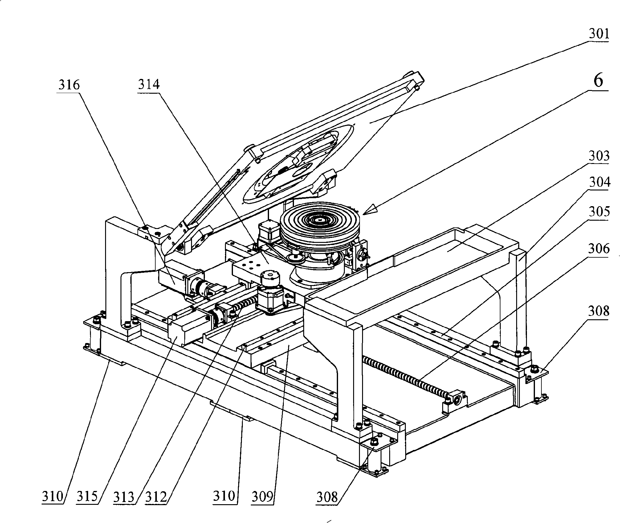
[0049] The fully automatic wafer testing method includes: a cassette placement frame 7 for carrying a wafer cassette 103; a wafer detection sensor 10 for recording the position and quantity of wafers in the cassette; taking a wafer clamp 205 for handling Wafer; the suction cup device 209 arranged on the top of the detection shaft 208 is used to rotate the wafer; the optical sensor mounting plate 11 is used to place the optical sensor for detecting the eccentricity of the wafer; the optical system is used to produce different multiples of the wafer Imaging; image acquisition device, used to obtain wafer images; computer, used to process image data and motion data; motion control card connected with computer, used to control motor drive mechanism; motor drive mechanism, used to obtain motion instructions and drive motor.

[0050] Such as figure 1 , the host is ...


PUM


Abstract

The invention discloses a full automatic wafer test method and a device to realize the test method. The method includes the following steps: scanning a spool box, drawing chips, rough adjusting, sending the chips, accuracy alignment, testing and replacing the wafer. The device to realize the full automatic wafer test method consists of a chip placing and counting device arranged on a stander, a wafer transmission device arranged on a stander at one side of the chip placing and counting device, and a wafer test platform device arranged at one side of the wafer transmission device and matched with the transmission device. The method has the advantages of high efficiency, low test cost, high automation and accurate test result.

Description

technical field [0001] The invention belongs to the technical field of semiconductor testing, discloses a fully automatic wafer testing method, and also discloses equipment for realizing the testing method. Background technique [0002] Semiconductor IC testing technology is divided into chip testing and finished product testing according to different stages of IC manufacturing. The former is a die good or bad test performed by probes while the product is still in the wafer fabrication stage. Reducing the cost of testing has become the primary goal of developing IC testing, and the demand for smaller and more powerful chips is driving the development of the IC industry, as well as the development of IC design and testing. For system-on-chip (SOC) testing, its cost has accounted for almost half of the chip cost. The biggest challenge facing IC test equipment manufacturers in the future is how to reduce test costs. [0003] Improving test speed and testing intelligence is a...

Claims


Application Information

Patent Timeline
Patent Type & Authority Applications(China)
IPC IPC(8): G01R31/26G01R31/28H01L21/66
Inventor 巴雅日图陈仲宇周骅戴京东
Owner 无锡市易控系统工程有限公司
Why Eureka
Try Eureka