Image data analogue-digital conversion method and image sensor

A technology of image data and analog-to-digital conversion, which is applied in the direction of image communication, TV, and color TV components, etc., which can solve the problems of increased power consumption of digital modules, large chip noise, and image quality impact, and reduce power consumption and floor noise, power consumption reduction, and the effect of reducing the number of counts

Active Publication Date: 2013-04-17
长春长光辰芯微电子股份有限公司
View PDF6 Cites 16 Cited by
  • Summary
  • Abstract
  • Description
  • Claims
  • Application Information

AI Technical Summary

Problems solved by technology

Especially in high-resolution image sensors, this will lead to a large power consumption of the digital module of the sensor, which in turn will cause a lot of noise on the substrate of the chip
In addition, the power consumption of the digital module in this analog-to-digital conversion method will change with the intensity of the pixel light signal, which will cause the chip floor noise to change with the light intensity, which will have a relatively bad impact on the image quality.

Method used


Image

  • Image data analogue-digital conversion method and image sensor
  • Image data analogue-digital conversion method and image sensor
  • Image data analogue-digital conversion method and image sensor

Examples


Embodiment 1

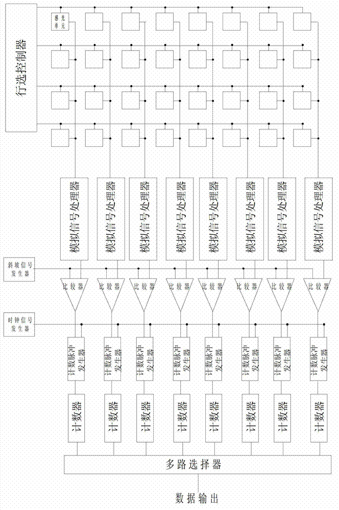
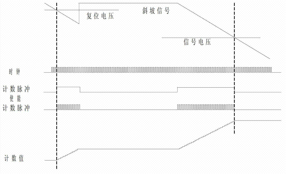
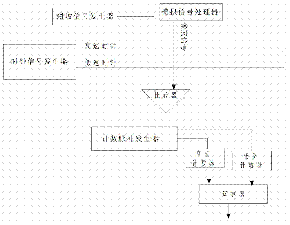
[0052] Such as Figure 5 As shown, it is one of the implementation methods of directly quantifying the difference between the pixel reset voltage and the signal voltage by using the image data analog-to-digital conversion method of the present invention. During the first quantization, a reset voltage is placed at the input of the comparator. The ramp signal starts at t0 and ends at t3. The output of the comparator starts to toggle at t1. The first falling edge of the low-speed clock after the comparator toggles occurs at t2. The first falling edge of the low-speed clock after the end of the ramp signal occurs at t4. The high-bit counter starts counting up from t2 and stops counting at t4. The low counter starts counting up at t1 and ends counting at t2. In the second quantization, the pixel signal voltage is placed at the input of the comparator. The ramp signal starts at t5 and ends at t9. The first falling edge of the low-speed clock after the start of the ramp signal ...

Embodiment 2

[0054] Figure 6 Another implementation method is to directly quantify the difference between the pixel reset voltage and the signal voltage by using the image data analog-to-digital conversion method of the present invention. During the first quantization, a reset voltage is placed at the input of the comparator. The ramp signal starts at t0 and ends at t4. The first falling edge of the low-speed clock after the start of the ramp occurs at t1. The output of the comparator starts to toggle at t2. The first falling edge of the low-speed clock after the comparator flips occurs at t3. The high-bit counter starts counting up from t1 and stops counting at t3. The low counter starts counting down at t2 and ends counting at t3. In the second conversion, the pixel signal voltage is placed at the input of the comparator. The ramp signal starts at t5 and ends at t8. The comparator toggles at t6. The first falling edge of the low-speed clock after the comparator flips occurs at t7....

Embodiment 3

[0056] Figure 7Another implementation method is to directly quantify the difference between the pixel reset voltage and the signal voltage by using the image data analog-to-digital conversion method of the present invention. During the first quantization, a reset voltage is placed at the input of the comparator. The ramp signal starts at t0 and ends at t4. The first falling edge of the low-speed clock after the start of the ramp occurs at t1. The output of the comparator starts to toggle at t2. The first falling edge of the low-speed clock after the comparator flips occurs at t3. The high-bit counter starts counting down from t1 and stops counting at t3. The low counter starts counting up at t2 and ends counting at t3. In the second conversion, the pixel signal voltage is placed at the input of the comparator. The ramp signal starts at t5 and ends at t9. The first falling edge of the low-speed clock after the start of the ramp signal to convert the pixel signal voltage o...


PUM


Abstract

The invention relates to an image data analogue-digital conversion method and an image sensor. A row selection controller of the image sensor is connected with light sensing unit arrays; each light sensing unit array is connected with a corresponding analogue signal processor through an array bus; each analogue signal processor is connected with a corresponding image data analogue-digital conversion device; and an arithmetic device of each image data analogue-digital conversion device is connected to a multi-path controller. The image data analogue-digital conversion devices adopt the image data analogue-digital conversion method disclosed by the invention to respectively carry out high-level and low-level counting through a low-speed clock pulse and a high-speed clock pulse, and finally obtain quantized pixel image data through operation treatment. The quantized pixel image data is read out of the image sensor array by array by the multi-path controller in a horizontal direction. According to the image data analogue-digital conversion method and the image sensor disclosed by the invention, power consumption of a sensor digital module and ground noises are greatly reduced; and meanwhile, the power consumption of the sensor is not changed along the light intensity so that the image quality of the sensor is further guaranteed.

Description

technical field [0001] The invention belongs to the technical field of image acquisition, and relates to an image data analog-to-digital conversion method and an image sensor. Background technique [0002] The image data analog-to-digital conversion method is mainly used to quantize the analog signal in the pixel array of the image sensor into a digital signal. Pixels in an image sensor convert light signals into analog electrical signals that can be used with some analog and digital signal processing to perform a variety of functions. [0003] Currently, as an alternative to traditional CCD image sensors, CMOS technology has been widely used in the design and manufacture of image sensors. It includes an array of photosensitive units called pixels and some auxiliary circuits for reading out the voltage signal of the array. Usually a pixel is composed of a light-sensitive photodiode and some transistors used to control the pixel. A typical pixel consists of a photodiode, a...

Claims


Application Information

Patent Timeline
IPC IPC(8): H04N5/357
Inventor 马成王欣洋
Owner 长春长光辰芯微电子股份有限公司
Why Eureka
Try Eureka