Electric field write-in and resistance readout solid-state storage component, storer and read-write method of storer
A component and resistance state technology, applied in the field of information storage, can solve the problems of high cost of SSD, limited storage performance, high power consumption of writing, etc., achieve fast writing speed, increase information storage capacity, and improve storage density.
- Summary
- Abstract
- Description
- Claims
- Application Information
AI Technical Summary
Problems solved by technology
Method used
Image
Examples
Embodiment 1
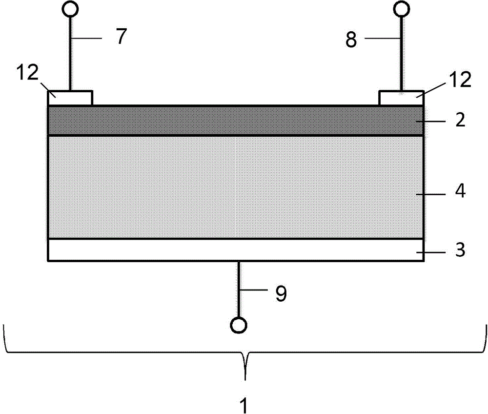
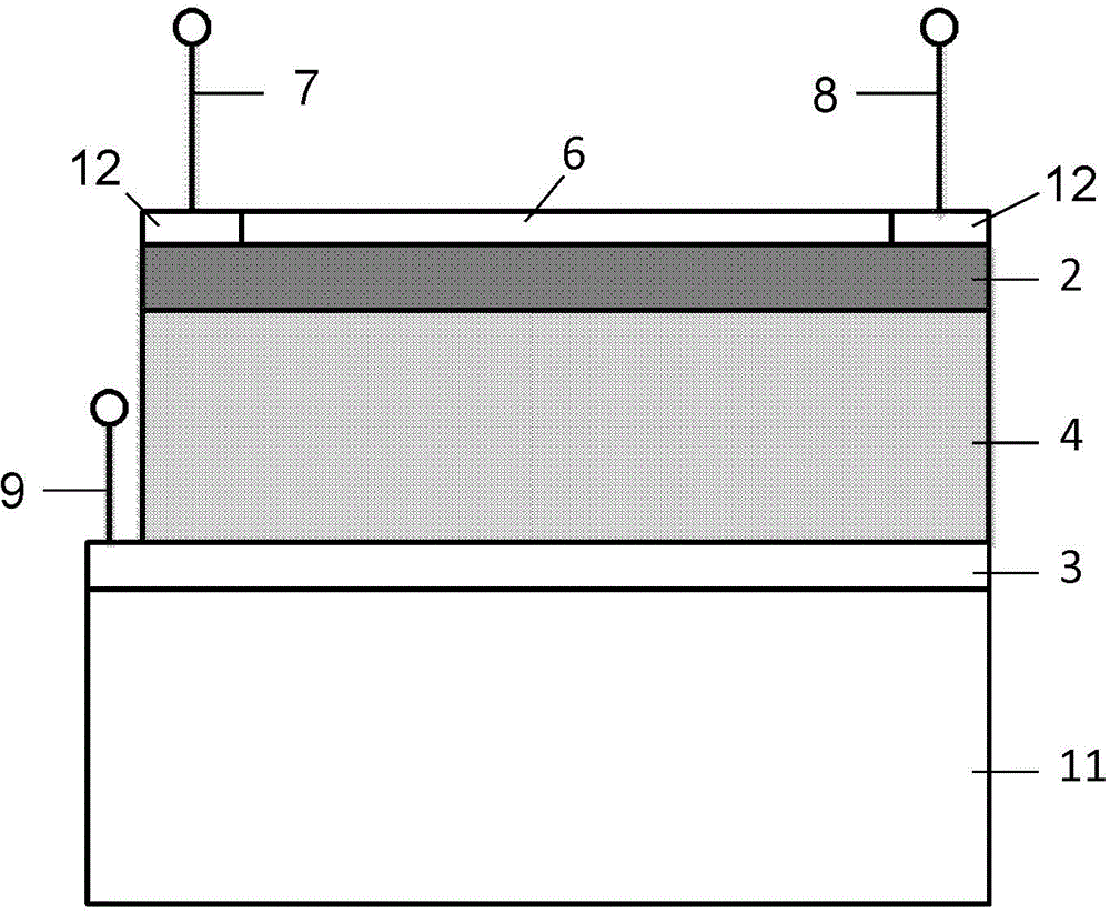
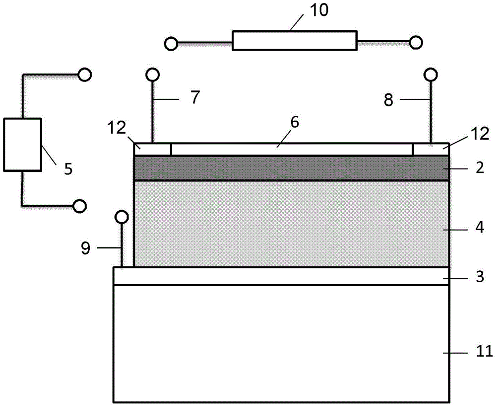
[0081] Embodiment 1 is a two-state solid-state storage device, see the attached Image 6 , in this embodiment, lead magnesium niobate-lead titanate (0.7Pb(Mg 2 / 3 Nb 1 / 3 )O 3 -0.3PbTiO 3 , referred to as: PMN-0.3PT, size: 5mm × 5.5mm × 0.55mm) grown on a solid solution single crystal substrate with a thickness of 80nm manganese oxide film La 2 / 3 Sr 1 / 3 MnO 3 (abbreviation: LSMO), PMN-0.3PT is used as the ferroelectric piezoelectric layer 4, LSMO is used as the resistance layer 2; Au is used as the bottom electrode layer 3 and the top electrode layer 12, and the writing electric field (V) is polarized through the electrode interconnection The PMN-0.3PT substrate induces the in-situ residual strain of the ferroelectric piezoelectric layer 4; correspondingly, the residual resistance state of the LSMO in the direction is read by the information readout device.
[0082] Figure 7 It is a chart of regulating the strain state of the piezoelectric layer by using an electric fie...
Embodiment 2
[0086] Further, based on the dependence of the strain of ferroelectric piezoelectric materials on the applied electric field history, we implemented a three-state solid-state memory using the LSMO / PMN-0.3PT heterojunction proposed in Example 1. In this example, we used the sample of Example 1.
[0087] attached Figure 10 Shown is the variation of the overall strain in the plane with the writing electric field. The strain is scanned from the positive (black and white circular lines) and negative (square lines) writing electric fields respectively, and after two different electric field scanning methods, three residual resistance states "0", "1" and "2" are generated. Specifically, similar to Embodiment 1, first carry out the forward scanning of the write electric field, we can obtain "0" and "1" states; then, reduce the write electric field (reach -E s ) to saturate and polarize the ferroelectric piezoelectric layer, scan negatively, increase the writing electric field and p...
PUM
 Abstract
Description
Claims
Application Information


