Organic light-emitting diode (OLED) panel packaging structure and packaging method

A packaging structure and panel technology, which is applied in the manufacturing of electrical components, electric solid-state devices, semiconductor/solid-state devices, etc., can solve the problems of crushing the connecting electrodes of organic light-emitting diodes, etc., to protect from damage, improve reliability, overcome crack effect

Inactive Publication Date: 2013-05-01
SICHUAN CCO DISPLAY TECH
View PDF3 Cites 9 Cited by
  • Summary
  • Abstract
  • Description
  • Claims
  • Application Information

AI Technical Summary

Problems solved by technology

[0006] The present invention is aimed at the existing OLED panel packaging structure and is applied to the package cover plate and/or substrate existing in the package of a large-area display panel (not less than 10 inches), when it is squeezed by external

Method used


Image

  • Organic light-emitting diode (OLED) panel packaging structure and packaging method
  • Organic light-emitting diode (OLED) panel packaging structure and packaging method
  • Organic light-emitting diode (OLED) panel packaging structure and packaging method

Examples


Embodiment Construction

[0022] The present invention will be further described below in conjunction with the accompanying drawings and specific embodiments.

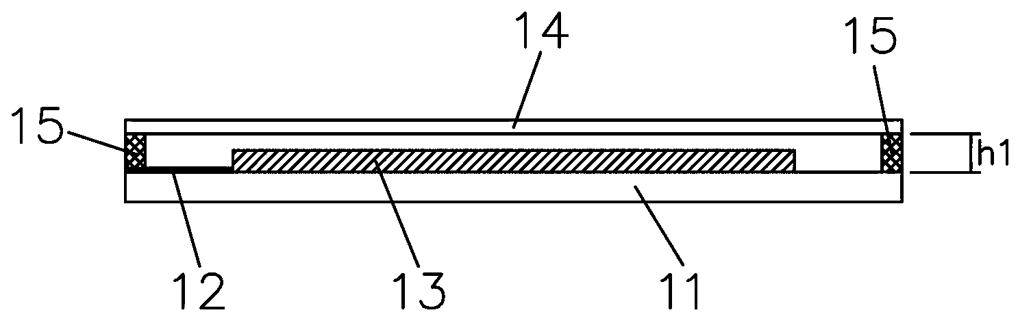
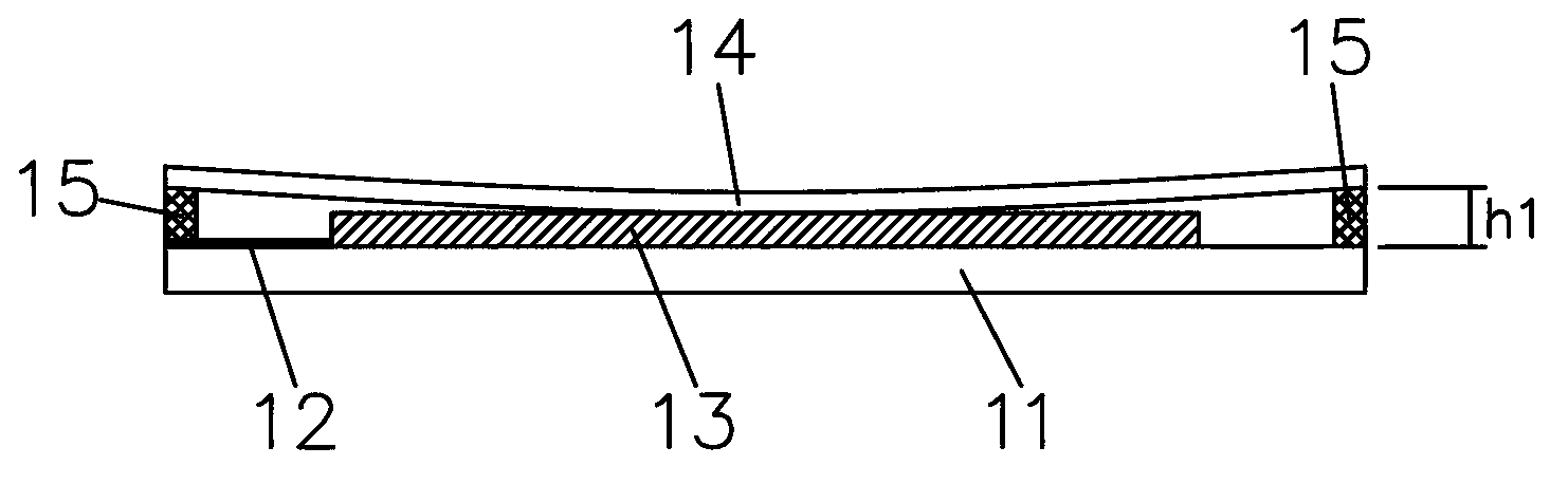
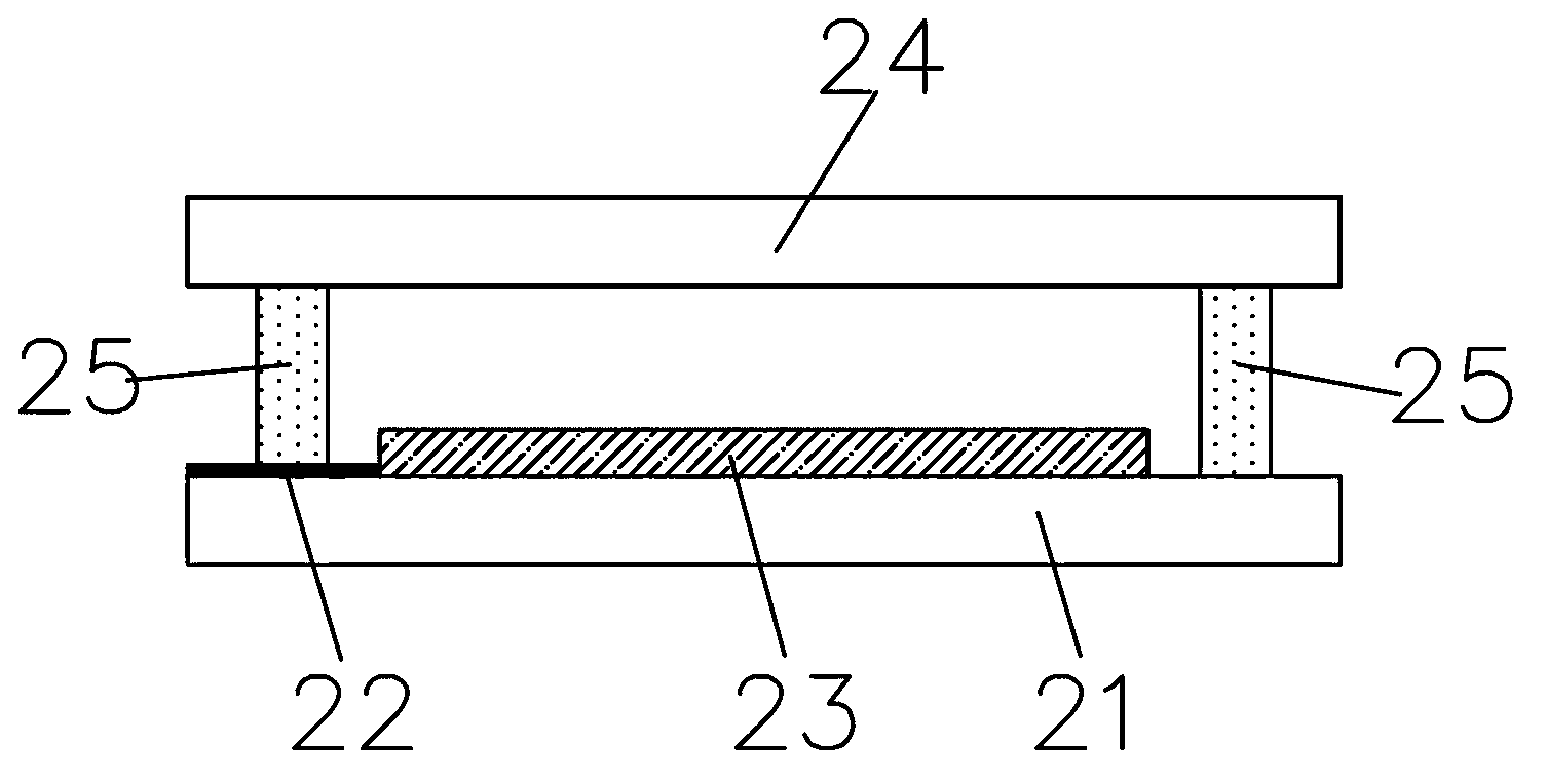
[0023] Such as Figure 2a Shown is a specific embodiment of an OLED panel packaging structure of the present invention, including a substrate 21, a connecting electrode 22, an organic light emitting diode 23 and a cover plate 24, wherein the connecting electrode 22 and the organic light emitting diode 23 are formed on the substrate 21; and The difference of the existing packaging structure is that the packaging structure of this embodiment also includes a glass wall 25 prepared in advance, and the glass wall is in the shape of a closed loop, such as Figure 2b As shown, the shape is consistent with the shape of the edge of the cover plate, and the glass wall is a low softening point glass containing a substance that absorbs specific light; in order to form the protection of the connection electrode 22 and the organic light emitting diode 23, be...


PUM

PropertyMeasurementUnit
Heightaaaaaaaaaa
Thicknessaaaaaaaaaa

Abstract

The invention provides an organic light-emitting diode (OLED) panel packaging structure and a packaging method for forming the packaging structure. The packaging structure comprises a base plate, a connecting electrode, an OLED, a cover plate and a glass wall. The glass wall is in a shape of a closed loop, and forms a closed cavity together with the base plate and the cover plate. The packaging method for forming the packaging structure comprises two steps of manufacturing the glass wall and aligning to bond. The invention has the beneficial effects that the cover plate can not easily contact with the OLED as the cover plate is stressed to deform, so that the OLED is effectively prevented from being damaged; meanwhile, after the glass wall is directly doped, the sealing reliability can be further enhanced by using the structure of the glass wall bonded with the base plate and the cover plate; and meanwhile the whole glass wall is doped, so that the phenomenon that fissures are generated caused by a temperature difference stress during an ordinary bonding procedure is prevented. The packaging structure is especially suitable for packaging OLED devices with large sizes, and the reliability in use of the OLED is improved.

Description

technical field [0001] The invention belongs to the technical field of organic light-emitting diode (OLED) display, relates to OLED packaging, and in particular to a packaging structure and packaging method of a large-sized OLED panel. Background technique [0002] Organic light-emitting diode (OLED) display is considered to be the next-generation flat panel display due to its all-solid-state, active light-emitting, high brightness, high contrast, ultra-thin and ultra-light, low power consumption, no viewing angle limitation, and wide operating temperature range. Display emerging application technology. However, part of the structure of OLED displays, especially the electrodes and organic materials located therein, are extremely sensitive to external environmental factors such as oxygen and moisture. In actual use, the device needs to be packaged to isolate the device from water vapor and oxygen to prolong the life of OLED Service life, if the packaging is not good, the com...

Claims


Application Information

Patent Timeline
IPC IPC(8): H01L51/52H01L51/56
Inventor 唐凡高昕伟邹成李园利高娟
Owner SICHUAN CCO DISPLAY TECH
Why Eureka
Try Eureka