


Quick Research
Generate reliable direction feasibility study reports for your R&D in just a few steps.

Technical Q&A
Discover and master advanced knowledge NOW. Basics, ideas, possibilities, all at once.

Find Solutions
As an expert in R&D theories, this can generate solutions to your technical problems instantly.

Evaluate Feasibility
Analyze your overall solution with one click, know your potential R&D risks in advance.

Monitor Landscape
Get weekly tech updates, stay abreast of the latest tech innovations and key insights.
Nitride semiconductor light-emitting element and manufacturing method therefor
一种氮化物类、发光元件的技术,应用在半导体器件、电气元件、电路等方向,能够解决发光效率降低、消耗电力增大等问题,达到提高发光效率的效果
- Summary
- Abstract
- Description
- Claims
- Application Information
AI Technical Summary
Problems solved by technology
Method used
Image

Examples
Embodiment Construction
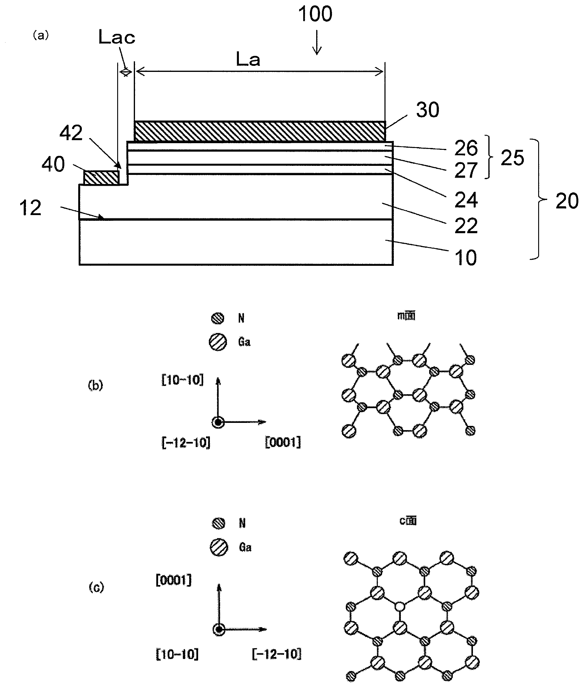
[0037] In general, in a c-plane LED, when the current is increased to obtain a large output, the injected carriers overflow from the active layer, so that the luminous efficiency decreases. In order to prevent this overflow, it may be considered to reduce the carrier density of the active layer by increasing the thickness of the active layer. This is because if the current injected into the active layer is constant, the more the volume of the active layer increases, the more the number of carriers contained in the unit volume inside the active layer decreases, and overflow is suppressed. However, in the case of a c-plane LED, even if the thickness of the active layer is increased, the luminous efficiency decreases on the contrary due to the existence of the piezoelectric field.
[0038] Therefore, in the c-plane LED of the prior art, the carrier density in the active layer is reduced not by increasing the thickness of the active layer but by increasing the chip area. Since th...
PUM
 Abstract
Description
Claims
Application Information
 - R&D Engineer
- R&D Manager
- IP Professional
- Industry Leading Data Capabilities
- Powerful AI technology
- Patent DNA Extraction
Browse by: Latest US Patents, China's latest patents, Technical Efficacy Thesaurus, Application Domain, Technology Topic, Popular Technical Reports.
© 2024 PatSnap. All rights reserved.Legal|Privacy policy|Modern Slavery Act Transparency Statement|Sitemap|About US| Contact US: help@patsnap.com