Layer structure comprising electrotechnical components
An electrotechnical technology and layer structure technology, applied in the direction of electric solid devices, electrical components, semiconductor devices, etc., can solve the problems of interference and sensitive maintenance, and achieve the effect of low price and simple method
Inactive Publication Date: 2013-05-01
BAYER IP GMBH
View PDF22 Cites 0 Cited by
- Summary
- Abstract
- Description
- Claims
- Application Information
AI Technical Summary
Problems solved by technology
The combinations of illuminated switches known from the prior art consisting of separate elements have the disadvantage that they are expensive to provide and are sensitive to disturbances and maintenance due to the use of mechanical parts for the switches
[0010] ACPEL film has the disadvantage that it requires an electrical supply consisting of high AC voltage (typically 110V) at high frequency (typically 400Hz)
OLEDs and PLEDs (PLED=polymeric light emitting diode) do not have the last-mentioned disadvantages of LEDs, but OLEDs and PLEDs are extremely sensitive to oxygen and moisture
Method used
View moreImage
Smart ImageViewing Examples
Examples
Embodiment Construction
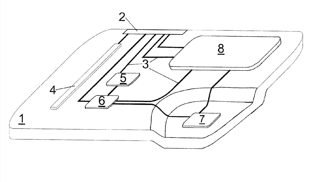
[0120] figure 1 A layer structure is shown, comprising a substrate 1 , electrical plug contacts 2 , electrical connections 3 , antenna 4 , sensor 5 , switch 6 , LEC 7 and battery 8 . As can be seen, the layer structure is three-dimensionally deformed in such a way that the LEC 7 is arranged on a deeper level with respect to all other components 2 - 6 . Currently, only electrical connections 3 are arranged at the transition between the main level of the layer structure and the deeper level of the LEC 7 . In principle, however, it is also possible to arrange the further described components on the three-dimensionally deformed transition region between the deeper level and the remaining levels of the layer structure.
Login to View More PUM
 Abstract
The layer structure has a substrate (1), a light emitting electrochemical cell (7) and an eletrotechnical component selected from the group that is made of an antenna (4), a switch, a sensor (5), a battery (8), photovoltaic cell, an actuator and an energy converter. The light emitting electrochemical cell and the component are formed on the substrate. The layer structure has a three-dimensional area. An independent claim is also included for a method for manufacturing a layer structure.
Description
technical field [0001] The subject of the invention is a layer structure comprising a substrate, at least one LEC (Light Emitting Electrochemical Cell) and at least one other electrotechnical device, a method for producing the layer structure, and for forming small and large displays and control elements and their application for constituting housing elements for mobile or stationary electronic equipment or small or large household appliances or for constituting keyboard systems without movable parts. Background technique [0002] In many technical fields there is a need to equip electrical or electronic devices with "light" components, ie lighting devices or displays. This can be, for example, a background lighting of the switch, which displays the position and / or the on / off state of the switch, or a display of the mobile radio device, which illuminates when the antenna of the mobile radio device receives a signal. In addition to switches or antennas, other electrotechnica...
Claims
Login to View More Application Information
Patent Timeline
 Patent Type & Authority Applications(China)
IPC IPC(8): H01L51/50H01L51/00H10K99/00
CPCH01L51/56H01L2251/5338H01L51/0096H05K1/16H01L27/3225H01L51/5032H05K2201/10106Y02B10/10Y02E10/50H01L51/0097Y02E10/549Y02P70/50H10K77/10H10K77/111H10K50/135H10K2102/311H10K59/00H10K71/00
Inventor R.孔茨W.黑德里希C.贝内克
Owner BAYER IP GMBH

