A kind of preparation method of high melting point lead-free solder for electronic packaging

A lead-free solder, electronic packaging technology, used in manufacturing tools, welding equipment, metal processing equipment and other directions, can solve the problem of under-recognized, achieve the advantages of mechanical properties, easy to obtain, and good economy.

Active Publication Date: 2016-07-06
CHONGQING UNIVERSITY OF SCIENCE AND TECHNOLOGY
View PDF6 Cites 0 Cited by
  • Summary
  • Abstract
  • Description
  • Claims
  • Application Information

AI Technical Summary

Problems solved by technology

Relevant foreign research institutions have invested a lot of manpower and material resources in research in this area, but domestic research in this area has not yet received attention

Method used


Image

  • A kind of preparation method of high melting point lead-free solder for electronic packaging
  • A kind of preparation method of high melting point lead-free solder for electronic packaging
  • A kind of preparation method of high melting point lead-free solder for electronic packaging

Examples


Embodiment 1

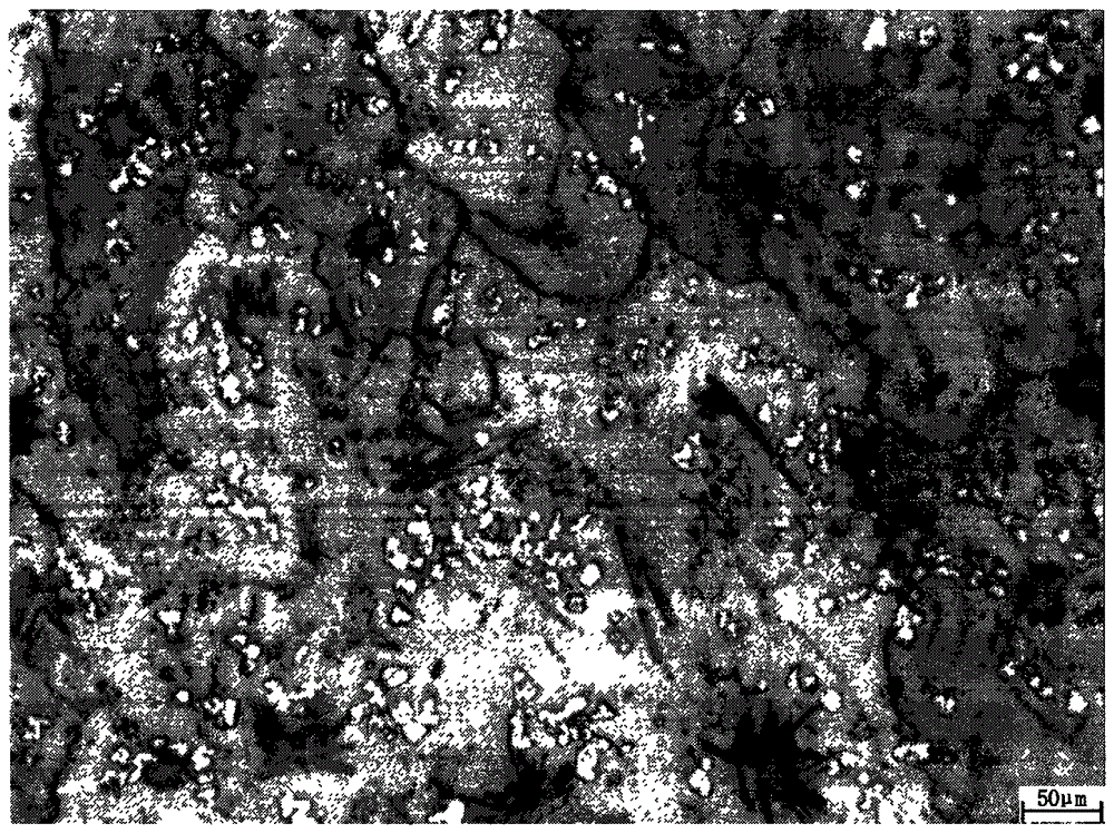
[0043] A high melting point lead-free solder for electronic packaging, the chemical composition of the solder is: 88wt% Bi, 10wt% Ag, 2wt% Cu, figure 1 It is the metallographic structure diagram of embodiment 1.

Embodiment 2

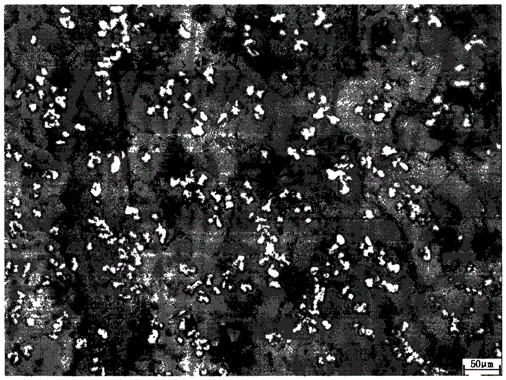
[0045] A high melting point lead-free solder for electronic packaging, the chemical composition of the solder is: 89wt% Bi, 10wt% Ag, 1wt% Cu, figure 2 It is the metallographic structure diagram of embodiment 2.

Embodiment 3

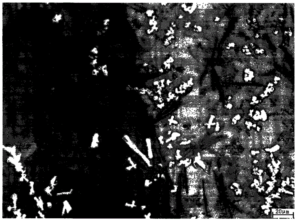
[0047] A high melting point lead-free solder for electronic packaging, the chemical composition of the solder is: 89.5wt% Bi, 10wt% Ag, 0.5wt% Cu, image 3 It is the metallographic structure diagram of embodiment 3.

[0048] From Figure 1-3 It can be seen that the microstructure of Bi-10Ag-0.5Cu, Bi-10Ag-1Cu, Bi-10Ag-2Cu solder consists of Bi phase, Bi-Ag eutectic structure, bright white dendritic primary crystal Ag and lath-like Cu phase composition. After adding a small amount of Cu, the biggest change in the microstructure of Bi-Ag-Cu and Bi-Ag is the formation of lath-like Cu phases in the structure, which are dispersed in the alloy system, and a small part sometimes gathers into a scallop shape. The morphology of the hypereutectic structure has a great influence.


PUM

PropertyMeasurementUnit
melting pointaaaaaaaaaa
shear strengthaaaaaaaaaa
surface tensionaaaaaaaaaa

Abstract

The invention relates to a high-melting-point lead free brazing filler metal used for electronic packaging. The high-melting-point lead free brazing filler metal used for electronic packaging is characterized in that the chemical composition of the brazing filler metal comprises, by weight, 88% to 89.5% of bismuth (Bi), 10% of silver (Ag) and 0.5% to 2% of copper(Cu). The melting temperature of the brazing filler metal is 260 DEG C to 270 DEG C. The shearing strength of the brazing filler metal is from 28 Mpa to 29.5 Mpa. Due to the fact that the brazing filler metal has an appropriate metlting temperature, the high-melting-point lead free brazing filler metal used for electronic packaging is large in potential to be a substituted brazing filler metal for a high-lead brazing filler metal.

Description

technical field [0001] The invention relates to a preparation method of lead-free solder for electronic packaging. Background technique [0002] With the continuous development of modern electronic products in the direction of miniaturization and multi-function, the density of electronic packaging is getting higher and higher, and the service environment (high temperature, high heat, high humidity, etc.) of new semiconductor chips and other electronic components is becoming increasingly severe. Therefore, the demand for high-temperature interconnect materials for electronic packaging will increase. In addition, the exemption period for high-lead solder is coming soon, and the development of suitable lead-free solder that can replace high-lead and high-melting-point solder has attracted much attention and needs to be solved urgently. Relevant foreign research institutions have invested a lot of manpower and material resources in this area of ​​research, but domestic research...

Claims


Application Information

Patent Timeline
Patent Type & Authority Patents(China)
IPC IPC(8): B23K35/26B23K35/40
Inventor 尹立孟尹建国夏文堂姚宗湘
Owner CHONGQING UNIVERSITY OF SCIENCE AND TECHNOLOGY
Why Eureka
Try Eureka