Tunable array waveguide grating based on liquid crystal waveguides

An arrayed waveguide grating and arrayed waveguide technology, which is applied in the directions of light guides, optics, optical components, etc., can solve the problems of high cost, poor performance consistency, complicated preparation process of tunable arrayed waveguide gratings, etc., and achieves good performance consistency and simple structure. , to achieve the effect of tunable performance

Active Publication Date: 2014-08-27
HUAZHONG UNIV OF SCI & TECH
View PDF5 Cites 0 Cited by
  • Summary
  • Abstract
  • Description
  • Claims
  • Application Information

AI Technical Summary

Problems solved by technology

[0005] The invention provides a tunable arrayed waveguide grating based on liquid crystal waveguide, which solves the problems of complex preparation process, high cost and poor performance consistency of the existing tunable arrayed waveguide grating

Method used


Image

  • Tunable array waveguide grating based on liquid crystal waveguides
  • Tunable array waveguide grating based on liquid crystal waveguides
  • Tunable array waveguide grating based on liquid crystal waveguides

Examples


Embodiment 1

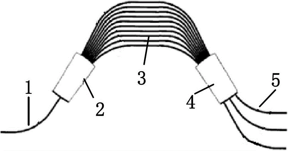
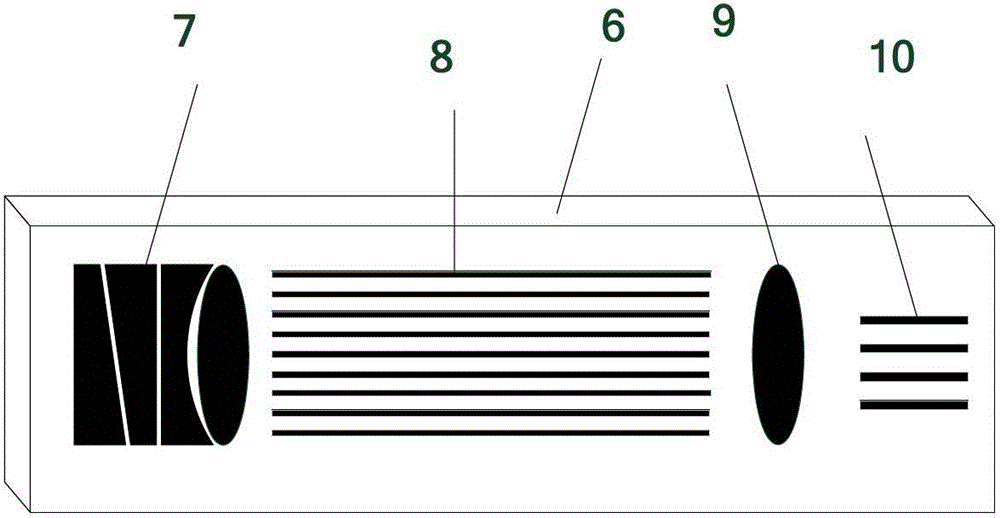
[0040] The gap between each part of the input coupling region 7 , the arrayed waveguide region 8 , the output coupling region 9 and the output waveguide region 10 is 300 μm;

[0041] The first right-angled trapezoidal prism-shaped electrode 7-1 and the second right-angled trapezoidal prism-shaped electrode 7-2 have an upper side length of 100 μm, a length ratio of the upper and lower sides of 1:4, and a height of 2000 μm.

[0042] The concave lens-shaped electrode 7-3 has an upper and lower side length of 400 μm, a height of 2000 μm, and a focal length of 500 μm.

[0043] The first convex lens shape electrode 7-4, height 2000μm, focal length 500μm,

[0044] The gap between the first right-angled trapezoidal prism-shaped electrode 7-1, the second right-angled trapezoidal prism-shaped electrode 7-2, the concave lens-shaped electrode 7-3 and the first convex lens-shaped electrode 7-4 is 20 μm;

[0045] The arrayed waveguide region 8 is composed of 80 parallel straight electrodes...

Embodiment 2

[0051] The gap between each part of the input coupling region 7 , the arrayed waveguide region 8 , the output coupling region 9 and the output waveguide region 10 is 50 μm;

[0052] The first right-angled trapezoidal prism-shaped electrode 7-1 and the second right-angled trapezoidal prism-shaped electrode 7-2 have an upper side length of 10 μm, a length ratio of the upper and lower sides of 1:2, and a height of 50 μm.

[0053] The concave lens-shaped electrode 7-3 has an upper and lower side length of 20 μm, a height of 50 μm, and a focal length of 100 μm.

[0054] The first convex lens-shaped electrode 7-4, height 50μm, focal length 100μm,

[0055] The gap between the first right-angled trapezoidal prism-shaped electrode 7-1, the second right-angled trapezoidal prism-shaped electrode 7-2, the concave lens-shaped electrode 7-3 and the first convex lens-shaped electrode 7-4 is 5 μm;

[0056] The arrayed waveguide region 8 is composed of 10 parallel straight electrodes, each of...

Embodiment 3

[0062] The gap between each part of the input coupling region 7 , the arrayed waveguide region 8 , the output coupling region 9 and the output waveguide region 10 is 100 μm;

[0063] The first right-angled trapezoidal prism-shaped electrode 7-1 and the second right-angled trapezoidal prism-shaped electrode 7-2 have an upper side length of 50 μm, a length ratio of the upper and lower sides of 1:3, and a height of 1000 μm.

[0064] The concave lens-shaped electrode 7-3 has an upper and lower side length of 150 μm, a height of 1000 μm, and a focal length of 100.

[0065] The first convex lens shape electrode 7-4, height 1000μm, focal length 100μm,

[0066] The gap between the first right-angled trapezoidal prism-shaped electrode 7-1, the second right-angled trapezoidal prism-shaped electrode 7-2, the concave lens-shaped electrode 7-3 and the first convex lens-shaped electrode 7-4 is 10 μm;

[0067] The arrayed waveguide region 8 is composed of 50 parallel straight electrodes, ea...


PUM

PropertyMeasurementUnit
lengthaaaaaaaaaa
thicknessaaaaaaaaaa
lengthaaaaaaaaaa

Abstract

The invention relates to a tunable array waveguide grating based on liquid crystal waveguides, and belongs to integrated waveguide optical devices. The problems that an existing tunable array waveguide grating is complex in preparation technology, relatively high in cost and relatively poor in consistency of performance are solved. The tunable array waveguide grating based on the liquid crystal waveguides comprises an input coupled area, an array waveguide area, an output coupled area and an output waveguide area, wherein the input coupled area, the array waveguide area, the output coupled area and the output waveguide area are arrayed in sequence on a light path, the input coupled area is formed by a first right trapezoid prism-shaped electrode, a second right trapezoid prism-shaped electrode, a concave-lens-shaped electrode and a first convex-lens-shaped electrode, the array waveguide area is formed by N parallel vertical-bar-shaped electrodes, the output coupled area is formed by second convex-lens-shaped electrodes, and the output waveguide area is formed by M parallel vertical-bar-shaped electrodes. The electrodes in various shapes are all plated on the upper surface of a liquid crystal layer of a liquid crystal waveguide. The tunable array waveguide grating based on the liquid crystal waveguides is simple in structure, easy to manufacture and low in cost, the electrooptic effect of the liquid crystal layer is used to achieve tunable performance, and the tunable array waveguide grating based on the liquid crystal waveguides is beneficial for demultiplexing wave band frequency tuning.

Description

technical field [0001] The invention belongs to an integrated waveguide optical device, in particular to a tunable arrayed waveguide grating based on a liquid crystal waveguide. Background technique [0002] Arrayed waveguide grating (AWG for short), as one of the most important optical devices in optical fiber communication network, has gradually moved from the laboratory stage to the commercial stage since it was proposed by Smit in 1988. like figure 1 As shown, the AWG of the traditional structure is generally composed of five parts: input waveguide 1 , input free transmission region 2 , array waveguide 3 , output free transmission region 4 , and output waveguide 5 . Since there is a certain optical path difference nΔL between adjacent waveguides in the arrayed waveguide, the light of each wavelength will produce different phase differences, thereby realizing the function of grating dispersion. The function of AWG is to separate the light of each wavelength in the compo...

Claims


Application Information

Patent Timeline
Patent Type & Authority Patents(China)
IPC IPC(8): G02B6/293G02F1/1343
Inventor 张敏明戴竞刘德明
Owner HUAZHONG UNIV OF SCI & TECH
Why Eureka
Try Eureka