Circuit protection device and its manufacturing method

A technology of circuit protection and manufacturing method, which is applied in the direction of resistors with positive temperature coefficients, resistance terminals/electrodes, etc., can solve the problems of affecting the effective use area of ​​devices, shrinking the size of circuit protection devices, occupying functional areas, etc., and achieving improvement Effective use of area, small device size, and the effect of avoiding waste

Inactive Publication Date: 2013-05-08
RAYCHEM ELECTRONICS (SHANGHAI ) LTD
View PDF6 Cites 4 Cited by
  • Summary
  • Abstract
  • Description
  • Claims
  • Application Information

AI Technical Summary

Problems solved by technology

[0004] for Figure 1a and 1b As shown in the circuit protection device, its terminal electrodes 105a, 105b need to communicate with the regions located on both sides of the PTC thermosensitive material layer 101 through the via hole 106, and the via hole 106 will occupy the functional area (Active Area) of the PTC thermosensitive material layer 101. ), thus affecting the effective utilization area of ​​the device
In addition, in order to form the via hole 106, the metal plating layer 103 needs to be etched to form a via hole corresponding to the via hole 106. This drilling process limits the further reduction of the size of the circuit protection device.

Method used


Image

  • Circuit protection device and its manufacturing method
  • Circuit protection device and its manufacturing method
  • Circuit protection device and its manufacturing method

Examples


Embodiment Construction

[0016] The making and using of the embodiments are discussed in detail below. It should be understood, however, that the specific embodiments discussed are merely illustrative of specific ways to make and use the invention, and do not limit the scope of the invention.

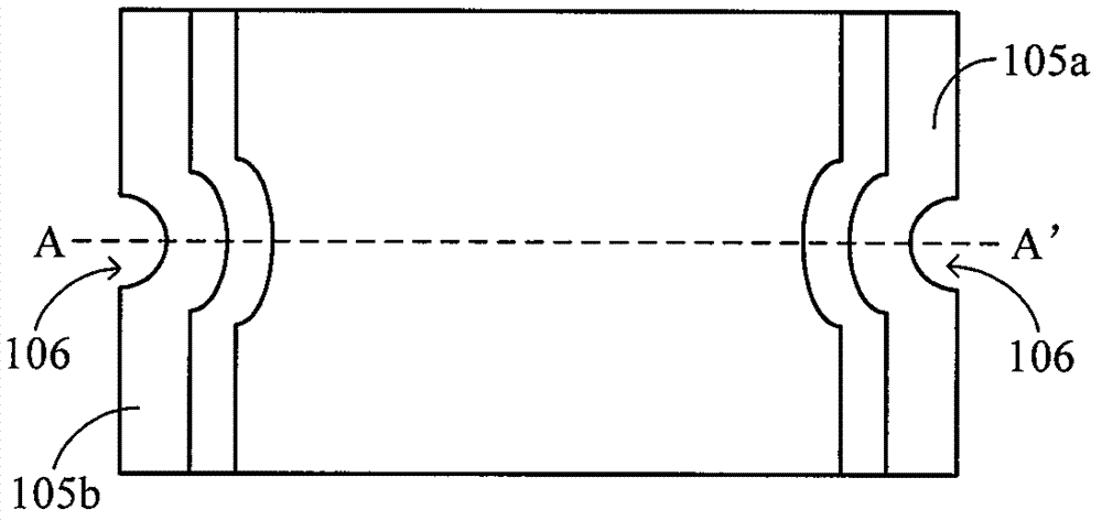
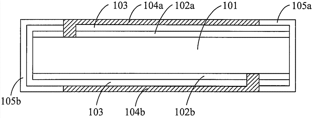
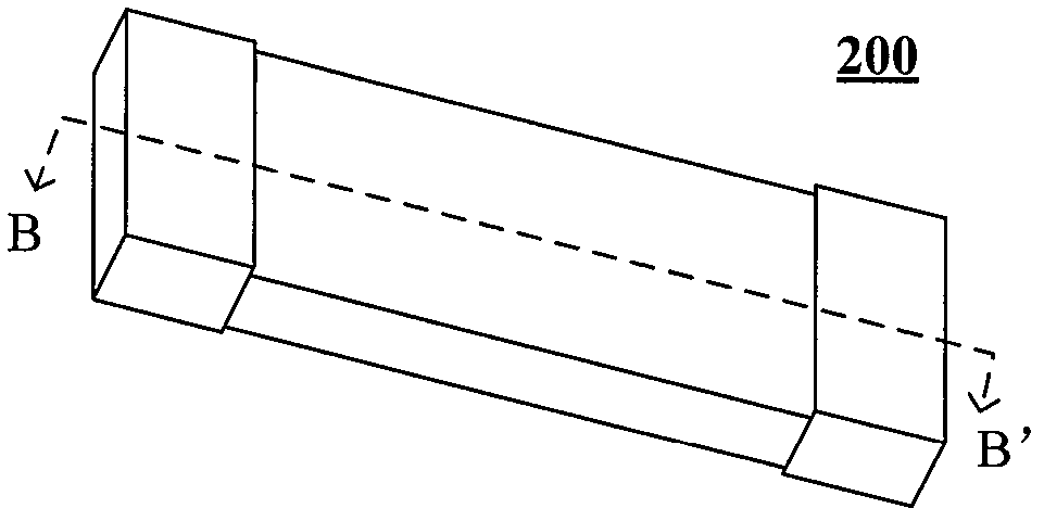
[0017] Figure 2a and Figure 2b A circuit protection device 200 according to a first embodiment of the present invention is shown. in, Figure 2a is a schematic perspective view of the circuit protection device 200, Figure 2b is along Figure 2a Schematic cross-sectional view in the direction of BB'. Next, combine Figure 2a and Figure 2b The circuit protection device 200 of the first embodiment of the present invention will be described.

[0018] Such as Figure 2a and Figure 2b As shown, the circuit protection device 200 includes:

[0019] A heat-sensitive material layer 201 with a positive temperature coefficient, the heat-sensitive material layer 201 has an opposite first surface 202 and a se...


PUM


Abstract

The invention discloses a circuit protection device, which includes: a positive temperature coefficient heat-sensitive material layer, which consists of a first face and an opposite second face, as well as a first end face and an opposite second end face, with the first face comprising a first area adjacent to the first end face and a second area adjacent to the first area, and the second face comprising a third area adjacent to the second end face and a fourth area adjacent to the third area; a first electrode layer, which covers the first area; a second electrode layer, which covers the third area; a first terminal electrode, which is located on the first end face and is connected to the first electrode layer; a second terminal electrode, which is positioned on the second end face and is connected to the second electrode layer; a first insulation layer, which covers at least a part of the second area and at least a part of the first electrode layer so as to isolate the first electrode layer and the second terminal electrode; and a second insulation layer, which covers at least a part of the fourth area and at least a part of the second electrode layer so as to isolate the second electrode layer and the first terminal electrode.

Description

technical field [0001] The invention relates to the technical field of electronic devices, and more specifically, the invention relates to a circuit protection device and a manufacturing method thereof. Background technique [0002] A thermistor is a resistor whose resistance value changes with temperature. According to different temperature coefficients, thermistors are generally divided into positive temperature coefficient (Positive Temperature Coefficient, PTC) thermistors and negative temperature coefficient (Negative Temperature Coefficient, NTC) thermistors. PTC thermistors increase in resistance as the temperature increases, while NTC thermistors decrease in resistance as the temperature increases. [0003] This positive temperature coefficient characteristic of PTC thermistor can be used for circuit protection. Figure 1a and Figure 1b That is, a circuit protection device using a PTC thermistor is shown, wherein, Figure 1a is a schematic top view of the circuit ...

Claims


Application Information

Patent Timeline
Patent Type & Authority Applications(China)
IPC IPC(8): H01C7/02H01C1/14
Inventor 何建成刘建勇潘杰兵袁飞
Owner RAYCHEM ELECTRONICS (SHANGHAI ) LTD
Why Eureka
Try Eureka