Method making back of wafer flat

A planarization method and technology on the back, applied in the direction of electrical components, semiconductor/solid-state device manufacturing, circuits, etc., can solve the problems of difficult control, particle pollution, scratches, etc., and achieve the effect of easy control

Active Publication Date: 2013-05-08
WUHAN XINXIN SEMICON MFG CO LTD
View PDF3 Cites 9 Cited by
  • Summary
  • Abstract
  • Description
  • Claims
  • Application Information

AI Technical Summary

Problems solved by technology

[0003] However, the planarization of its wafer backside is a huge challenge
At present, mechanical grinding is used to thin the back of the wafer, but there are many disadvantages in the use of mechanical grinding, for example, it is difficult to reduce the thickness of the wafer to 2um, and mechanical grinding is easy to cause defects, such as scratches, etc.
The main component of the edge of the wafer is silicon oxide. When trimming the wafer, the method of mechanical grinding is not easy to control and will cause particle pollution.

Method used


Image

  • Method making back of wafer flat
  • Method making back of wafer flat
  • Method making back of wafer flat

Examples


Embodiment Construction

[0022] The principles and features of the present invention will be described below with reference to the accompanying drawings. The examples cited are only used to explain the present invention, and are not used to limit the scope of the present invention.

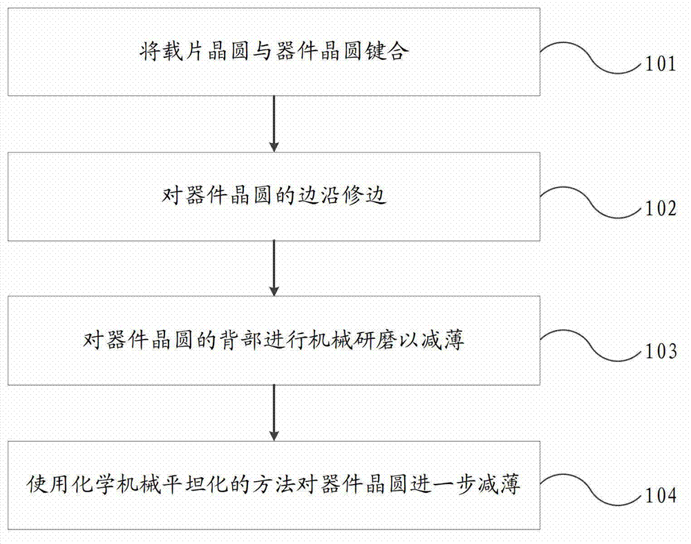
[0023] Such as figure 1 As shown, a method for flattening the back of a wafer includes the following steps:

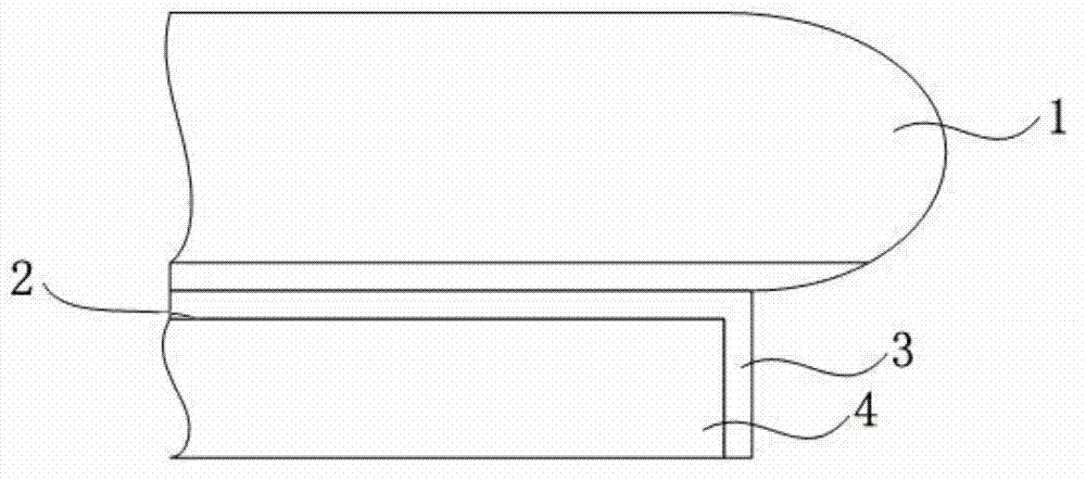
[0024] Step 101: bonding the carrier wafer 1 and the device wafer 2 through a bonding oxide, such as silicon dioxide;

[0025] Step 102: Trimming the device wafer 2 to make the edges of the device wafer 2 smooth;

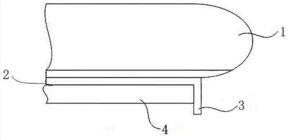
[0026] Step 103: Perform mechanical grinding on the back of the device wafer 2, which is the side opposite to the side bonded to the device wafer 2, and grind the device wafer 2 to the device wafer 2 The thickness is 25um~50um, the structure diagram of the finished product after grinding is as follows figure 2 Shown

[0027] Step 104: Process the back of the device wafer 2 by a chemical-mechanical planarization...


PUM


Abstract

The invention relates to the manufacture field of semiconductors, in particular to a method making a back of a wafer flat. The method comprises the following steps: a slide glass wafer is bonded with a device wafer through a bonding oxidizing material; the device wafer is deburred to enable edges of the device wafer to be smooth and evasive; the back of the device wafer is caught out mechanical lapping, and the thickness of the device wafer is lapped to be 25 microns -50 microns; the back of the device wafer is processed through a chemical method, and the thickness of the device wafer is further reduced to 2 microns-3 microns. Monox which has a hard character is etched through a chemical etching method. For a process with thickness requirements which is high in accuracy, chemical lapping is easier to control than the mechanical lapping, and particulate pollution cannot be polluted.

Description

Technical field [0001] The invention relates to the field of semiconductor manufacturing, in particular to a method for flattening the back of a wafer. Background technique [0002] The wafer thinning process has a wide range of applications in some advanced technologies, such as 3D IC (three-dimensional integrated circuit), back-illuminated image sensor and so on. The upper part of the wafer is used to conduct each wafer, and the polishing process is used on the back of the wafer (the surface opposite to the upper part), and the polishing includes mechanical polishing and chemical polishing. [0003] However, the flattening of the backside of the wafer is a huge challenge. At present, mechanical polishing is used to thin the back of the wafer, but mechanical polishing has many disadvantages. For example, it is difficult to reduce the thickness of the wafer to 2um, and mechanical polishing is likely to cause defects such as scratches. The main component of the edge of the wafer i...

Claims


Application Information

Patent Timeline
Patent Type & Authority Applications(China)
IPC IPC(8): H01L21/306
Inventor 李平
Owner WUHAN XINXIN SEMICON MFG CO LTD
Why Eureka
Try Eureka