
Efficient groove type insulated gate bipolar transistor IGBT
A bipolar transistor and trench technology, applied in semiconductor devices, electrical components, circuits, etc., can solve the problems of large resistance and low efficiency, and achieve the effect of reducing saturation voltage and increasing efficiency
- Summary
- Abstract
- Description
- Claims
- Application Information
AI Technical Summary
Problems solved by technology
Method used
Image

Examples
Embodiment 1
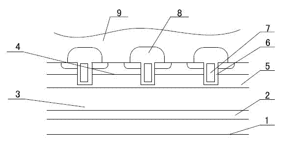
[0020] Example 1 trench 6 penetrates N + and P-type region P-body 4 in the N-layer structure
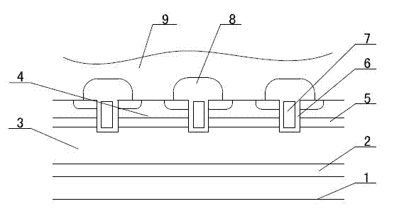
[0021] This high-efficiency trench insulated gate bipolar transistor IGBT consists of a main body P+Substrate 1, a first epitaxial buffer layer 2, a second epitaxial drift layer 3, an N layer, a P-type region P-body 4, and a third Layer epitaxial layer 5, trench 6, polysilicon 7, borophosphosilicate glass BPSG 8 and aluminum layer AL 9. From bottom to top: the bottom layer is the main body P+Substrate 1, the first layer of epitaxial buffer layer 2 above the main body P+Substrate 1, the second layer of epitaxial drift layer 3 and N above the first layer of epitaxial buffer layer 2 layer, P-type region P-body 4, third epitaxial layer 5, trench 6, polysilicon 7, borophosphosilicate glass BPSG 8 and aluminum layer AL 9. The main body P+Substrate1 is a heavily doped P-type substrate, and the groove 6 outside the polysilicon 7 only penetrates the N + And the P-body 4 of the P-type regio...
Embodiment 2
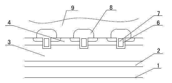
[0025] Embodiment 2 trench 6 is a through N + , P-type region P-body 4 and N-layer structure
[0026] The difference between this high-efficiency trench type insulated gate bipolar transistor IGBT and Embodiment 1 is that the trench 6 is a punch-through N + , P-type region P-body 4 and N-layer structure. All the other are the same as in Example 1. No longer.
[0027] The three-layer epitaxial layer of the present invention can also be applied to similar structures of other high-voltage devices.
PUM
 Abstract
Description
Claims
Application Information