
An igbt chip based on n-type injection layer and its manufacturing method

A manufacturing method and injection layer technology, applied in semiconductor/solid-state device manufacturing, electrical components, circuits, etc., can solve the problems of large chip terminal area size, large conduction loss, large saturation voltage, etc., achieve process compatibility, improve current ability, the effect of reducing the saturation voltage

Active Publication Date: 2017-02-08
STATE GRID CORP OF CHINA +2
View PDF3 Cites 0 Cited by
  • Summary
  • Abstract
  • Description
  • Claims
  • Application Information

AI Technical Summary

Problems solved by technology

The existing IGBT technology has the disadvantages of large saturation voltage and large conduction loss
In addition, the size of the terminal area of ​​the existing IGBT chip is large, which compresses the area of ​​the active area (that is, the area of ​​the effective chip). Compressing the size of the terminal area is also one of the development directions of the IGBT.

Method used


Image

  • An igbt chip based on n-type injection layer and its manufacturing method
  • An igbt chip based on n-type injection layer and its manufacturing method
  • An igbt chip based on n-type injection layer and its manufacturing method

Examples


Embodiment 1

[0053] Embodiment 1 of the manufacturing method of IGBT active region structure of the present invention see Figure 5 . Figure 5 Among them, the N-type injection layer 9 surrounds the P-base region 3, function 1, the horizontal and vertical dimensions of the P-base region are compressed, the distance between the P-base regions increases, the excess carrier concentration increases, and the saturation voltage decreases. Function 2, the channel length becomes shorter, the channel resistance becomes smaller, and the saturation voltage decreases. Function 3, the radius of curvature at the corner of the P-base region decreases, the breakdown voltage decreases, and there is a risk of breakdown. Among them, functions 1 and 2 are advantages, and function 3 is a disadvantage, which needs to be considered in compromise.

Embodiment 2

[0055] Example 2 of the manufacturing method of the IGBT active region structure of the present invention see Figure 6 . Figure 6 Among them, the N-type injection layer 9 surrounds the P-base region 3 and extends below the gate oxide layer 8 . Effect 1, compared with Example 1, the excess carrier field further increases, and the saturation voltage further decreases. Function 2, the channel length becomes shorter, the channel resistance becomes smaller, and the saturation voltage decreases. Function 3, the radius of curvature at the corner of the P-base region decreases, the breakdown voltage decreases, and there is a risk of breakdown. Effect 4, compared with Example 1, the number of N-type injection layer photolithography plates can be reduced, and the cost can be reduced. Among them, functions 1, 2, and 4 are advantages, and function 3 is a disadvantage, which needs to be considered in compromise. Implementation example 2 further enhances the current capability of the ...

Embodiment 3

[0057] Example 3 of the manufacturing method of the IGBT active region structure of the present invention see Figure 7 . Figure 7 In this example, compared with Embodiment 1, the N-type injection layer 9 surrounds the P-base region 3 and does not surround the corner of the P-base region. Advantages 1, 2 of embodiment 1 are therefore inherited, while disadvantage 3 of embodiment 1, namely the risk of breakdown, is avoided.

[0058] The terminal area is located in the edge area of ​​the IGBT chip and integrates the withstand voltage parameters of the IGBT chip. The terminal area includes a terminal basic unit; the terminal basic unit includes a field plate, a field limiting ring, a junction terminal extension protection module, a lateral variable doping Miscellaneous modules and resistive field plates, the terminal basic unit is used to reduce the curvature of the PN junction at the edge of the active region, the depletion layer extends laterally, and enhances the withstand v...


PUM


Abstract

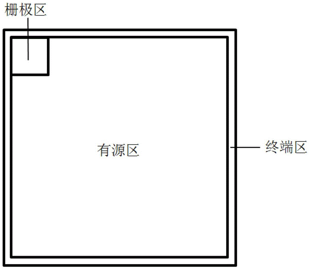
The invention relates to a semiconductor device technology, in particular to an insulated gate bipolar translator (IGBT) chip based on N-type injection layers and a manufacturing method thereof. The IGBT chip comprises an active area, a terminal area and a grid electrode area, wherein the N-type injection layers are arranged in the active area and the terminal area; the N-type injection layer in the active area comprises the following setting modes: the N-type injection layer encircles a P-base area; the N-type injection layer encircles the P-base area and extends to be below a grid oxidation layer, and the N-type injection layer encircles the P-base area and does not encircle the corner of the P-base area. The invention also provides a manufacturing method of the IGBT chip. The N-type injection layers are introduced when the IGBT is designed, so that the design of the terminal area is optimized, the size of the terminal area is reduced, the saturated voltage of the active area is reduced and the current capability of the chip is improved. The N-type injection layers are introduced under the premise of not influencing other properties of the IGBT chip, so that the proportion of each functional area of the IGBT chip is optimized and the current capability of the IGBT chip is improved.

Description

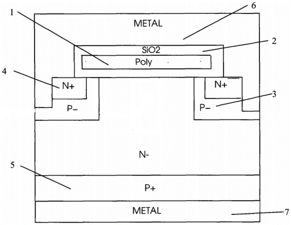
technical field [0001] The invention relates to semiconductor device technology, in particular to an IGBT chip based on an N-type injection layer and a manufacturing method thereof. Background technique [0002] IGBT (Insulated Gate Bipolar Transistor) has the advantages of both unipolar devices and bipolar devices, simple driving circuit, low power consumption and cost of control circuit, low saturation voltage, and low loss of the device itself. It is the development of high voltage and high current in the future. direction. [0003] IGBT is a three-terminal device, including front emitter, gate and back collector. For the cross-sectional view of the active area of ​​the IGBT chip, see figure 1 , including the emitter 6 on the front, the gate 1 and the collector 7 on the back. The surface is a MOSFET structure, and the back is a parasitic PNP tube structure. Among them: 1 polycrystalline, 2 oxide layer, 3P-base region, 4N+ emitter region, 5P+ collector region, 6 emitte...

Claims


Application Information

Patent Timeline
Patent Type & Authority Patents(China)
IPC IPC(8): H01L29/739H01L29/06H01L21/331
CPCH01L29/0615H01L29/66325H01L29/7393
Inventor 刘江包海龙张宇刘隽车家杰赵哿高明超金锐
Owner STATE GRID CORP OF CHINA
Learn More