Thin film transistor and its manufacturing method

A technology for thin film transistors and active regions, which is applied to transistors, semiconductor/solid-state device manufacturing, semiconductor devices, etc., can solve problems such as troublesome preparation processes and complex thin-film transistor structures, and achieves simple preparation methods, reduced saturation voltage, and threshold value. The effect of voltage drift reduction

Active Publication Date: 2017-12-15
BOE TECH GRP CO LTD
View PDF5 Cites 0 Cited by
  • Summary
  • Abstract
  • Description
  • Claims
  • Application Information

AI Technical Summary

Problems solved by technology

[0006] The present invention aims at the problems of complex structures and cumbersome preparation processes of existing double-gate or floating-gate thin film transistors, and provides a thin film transistor with good performance and simple preparation process and its preparation method

Method used


Image

  • Thin film transistor and its manufacturing method
  • Thin film transistor and its manufacturing method
  • Thin film transistor and its manufacturing method

Examples


Embodiment 1

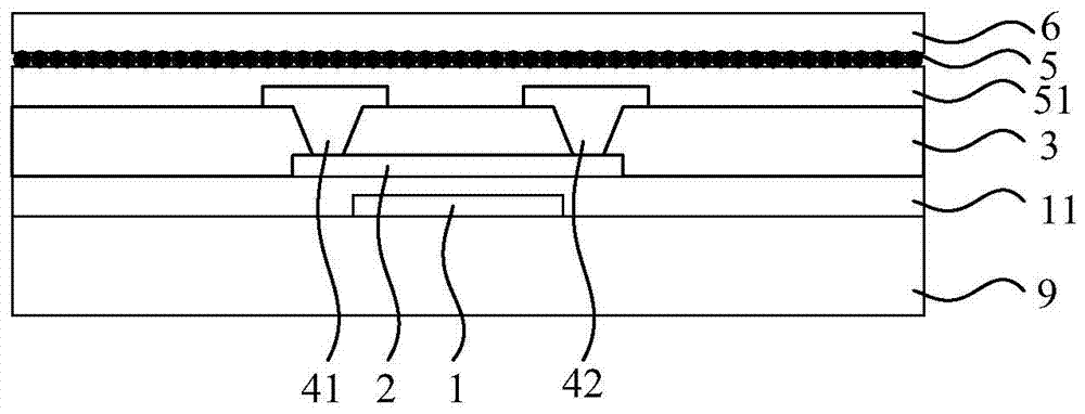
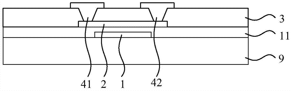
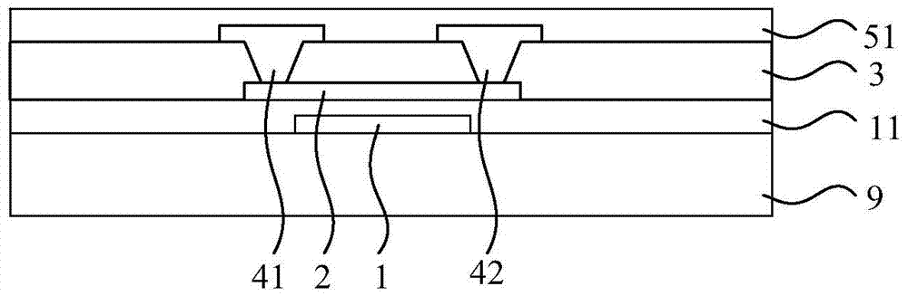
[0030] Such as Figure 1 to Figure 4 As shown, this embodiment provides a thin film transistor.

[0031] Specifically, the thin film transistor can be used in array substrates of liquid crystal display devices, organic light emitting diode display devices, and the like. Of course, it is also feasible if the thin film transistor is used for other purposes.

[0032] Specifically, the above thin film transistors include:

[0033] active zone 2;

[0034] The gate 1 and the gate insulating layer 11, the gate 1 and the gate insulating layer 11 are arranged on one of the upper and lower sides of the active region 2;

[0035] The floating gate layer 5 disposed on the other side of the upper and lower sides of the active region 2, the floating gate layer 5 includes quantum dots (preferably composed of quantum dots).

[0036] That is, if figure 1 As shown, the thin film transistor includes an active region 2 composed of a semiconductor material, preferably amorphous indium gallium ...

Embodiment 2

[0073] This embodiment provides an array substrate, which includes the above thin film transistor.

[0074] This embodiment provides a display device, which includes the above-mentioned array substrate.

[0075] Specifically, the display device can be any product or component with a display function such as a liquid crystal display panel, electronic paper, OLED panel, mobile phone, tablet computer, television, monitor, notebook computer, digital photo frame, and navigator.


PUM


Abstract

The invention provides a thin-film transistor and a preparation method thereof, belongs to the technical field of thin-film transistors, and can solve problems that an existing thin-film transistor with a double gate or floating gate structure is complex in structure and troublesome in preparation technology. The thin-film transistor comprises an active region; a gate electrode and a gate insulating layer which are arranged at one side of the upper and lower sides of the active region; and a floating gate layer which is arranged at the other side of the upper and lower sides of the active region and comprises quantum dots.

Description

technical field [0001] The invention belongs to the technical field of thin film transistors, and in particular relates to a thin film transistor and a preparation method thereof. Background technique [0002] Thin film transistors are important devices in array substrates of liquid crystal display devices, organic light emitting diode (OLED) display devices, and the like. Therefore, the performance of the thin film transistor will have a significant impact on the quality of the display device. [0003] In order to improve the stability of the threshold voltage of the thin film transistor, a thin film transistor with a "double gate" structure can be used; that is, there are interconnected gates on the upper and lower sides of the active area, so that the two gates can generate a double gate at the active area. The vertical electric fields cancel each other, so that the carriers are mainly concentrated in the middle of the active region, and the defects at the interface of t...

Claims


Application Information

Patent Timeline
Patent Type & Authority Patents(China)
IPC IPC(8): H01L29/786H01L21/336H01L29/423
CPCH01L29/42324H01L29/66742H01L29/78645
Inventor 徐晓娜
Owner BOE TECH GRP CO LTD
Why Eureka
Try Eureka