Heat conduction structure of patch power component on circuit board

A technology of power components and heat conduction structure, which is applied in the directions of printed circuit components, cooling/ventilation/heating transformation, etc., can solve the problems affecting the overall layout of electrical appliances, high power of SMD power components, and large circuit board volume, etc., to achieve production Low cost, large cooling area and large volume

Inactive Publication Date: 2013-05-08
WENZHOU SANLI ELECTRONICS TECH
View PDF6 Cites 4 Cited by
  • Summary
  • Abstract
  • Description
  • Claims
  • Application Information

AI Technical Summary

Problems solved by technology

The disadvantage is that the aluminum substrate or copper substrate of the metal substrate is more expensive than the general circuit board, and the aluminum substrate or copper substrate of the metal substrate can only place SMD components on one side
[0004] The other is to directly solder the SMD power element to the front of the heat-conducting copper block embedded in the circuit board, and then connect the heat-conducting copper block to the heat dissipation plate to facilitate heat dissipation (see "SMD High-Power SMD" disclosed in Chinese patent CN101556941B Component Heat Dissipation Structure" literature), its shortcomings: First, due to the high power of some SMD power components, larger heat-conducting copper blocks and heat dissipation plates must be used, resulting in larger circuit boards and affecting the performance of electrical appliances. The overall layout; the second is that due to the high power of some SMD power components, the metal shell of the SMD power component and the heat-dissipating aluminum plate or copper plate are prone to local overheating after welding, resulting in desoldering, which can easily lead to circuit failure

Method used


Image

  • Heat conduction structure of patch power component on circuit board
  • Heat conduction structure of patch power component on circuit board

Examples


Embodiment Construction

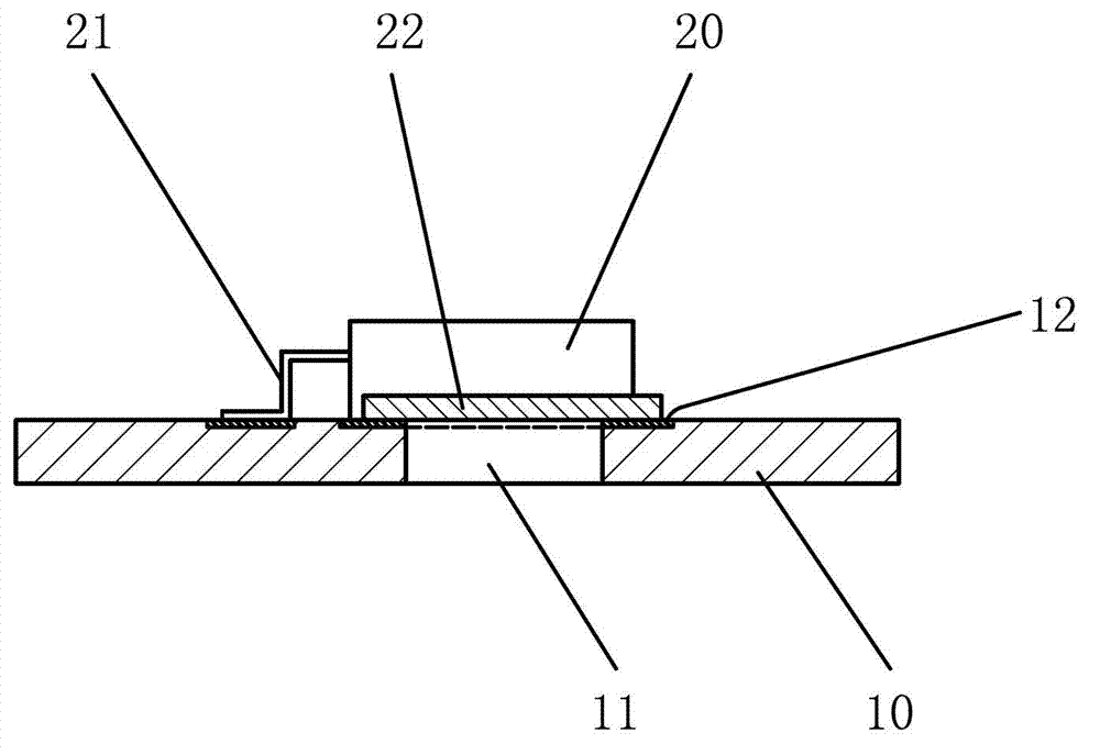
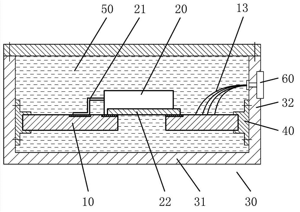
[0016] Below in conjunction with accompanying drawing, the present invention will be further described with specific embodiment, see figure 1 -2:

[0017] The thermal conduction structure of the SMD power component on the circuit board, the circuit board 10 is provided with a plurality of installation positions 12 for installing the SMD power component 20, and each installation position 12 for installing the SMD power component on the circuit board 10 is correspondingly provided with a through hole Through the through hole 11 of the circuit board 10 , a SMD power component 20 is mounted on each mounting position 12 of the circuit board 11 , and each electrode piece 21 of the SMD power component 20 is electrically connected to the corresponding circuit on the circuit board 10 .

[0018] The above-mentioned circuit board 10 is a circuit board of an insulating base material.

[0019] The above-mentioned through hole 11 is a round hole or a polygonal hole, and the area of ​​the t...


PUM


Abstract

The invention belongs to the technical field of patch power components and relates to a heat conduction structure of the patch power components on a circuit board. A plurality of installation positions for installing the patch power components are arranged on the circuit board, a through hole which penetrates the circuit board is formed in each installation position for installing each patch power component on the circuit board, a patch power component is installed on each installation position on the circuit board, and each electrode slice of each patch power component is electrically connected with a corresponding circuit on the circuit board. The heat conduction structure of the patch power components on the circuit board has the advantages that heat generated by the patch power components in the process of working is transmitted to the wall of a shell instantly by means of insulation heat conduction liquid and then dissipated into the air by means of heat dissipation slices on the wall of the shell. The heat conduction structure of the patch power components on the circuit board is rapid in heat dissipation, small in size, little in used raw material, low in cost, low in failure rate, and long in service life.

Description

technical field [0001] The invention belongs to the technical field of chip power components, in particular to a heat conduction structure of chip power components on a circuit board. Background technique [0002] At present, the connection structure between general SMD power components and circuit boards has the following structures [0003] A more common method is to attach the bottom cooling surface of the SMD power component to the aluminum substrate or copper substrate of the metal substrate. The disadvantage is that the aluminum substrate or copper substrate of the metal substrate is more expensive than the general circuit board, and the aluminum substrate or copper substrate of the metal substrate can only place SMD components on one side. [0004] The other is to directly weld the SMD power element to the front of the heat-conducting copper block embedded in the circuit board, and then connect the heat-conducting copper block to the heat dissipation plate to facilit...

Claims


Application Information

Patent Timeline
Patent Type & Authority Applications(China)
IPC IPC(8): H05K1/02H05K7/20
Inventor 陈夏新
Owner WENZHOU SANLI ELECTRONICS TECH
Why Eureka
Try Eureka