Manufacture method of semiconductor device provided with metal grid lamination

A manufacturing method and a metal gate technology, which are applied in the direction of semiconductor devices, etc., can solve problems such as poor filling effect and difficult filling of interlayer dielectric layer 17, and achieve the effect of small aspect ratio and simplified manufacturing process

Active Publication Date: 2013-05-22
SEMICON MFG INT (SHANGHAI) CORP
View PDF3 Cites 0 Cited by
  • Summary
  • Abstract
  • Description
  • Claims
  • Application Information

AI Technical Summary

Problems solved by technology

When the interlayer dielectric layer 17 is deposited in the above step S3, the interlayer dielectric layer 17 is difficult to fill between the gate structure 18a and the gate structure 18b, resulting in poor filling effect

Method used


Image

  • Manufacture method of semiconductor device provided with metal grid lamination
  • Manufacture method of semiconductor device provided with metal grid lamination
  • Manufacture method of semiconductor device provided with metal grid lamination

Examples


Embodiment Construction

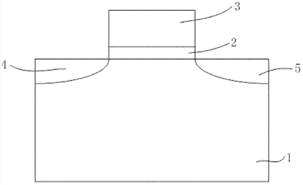
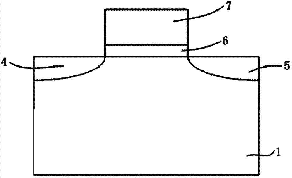
[0056] As mentioned above, the problem to be solved by the present invention is to provide a method for manufacturing a semiconductor device with metal gate stacks, so that the method can form polysilicon dummy gates with the tops at the same height, and then obtain the top at the same height. The high metal gate stack avoids a series of problems caused by the fact that the tops of the polysilicon dummy gates are not at the same height in the process of manufacturing the semiconductor device.

[0057] In the present invention, after the shallow trench isolation structure whose top is higher than the surface of the semiconductor substrate is formed on the semiconductor substrate, a filling layer is deposited on the semiconductor substrate formed with the shallow trench isolation structure, and the structure beyond the shallow trench isolation structure is removed. The filling layer on the top, by controlling the process accuracy when removing the filling layer, the surface of th...


PUM


Abstract

The invention provides a manufacture method of a semiconductor device provided with a metal grid lamination. The manufacture method of the semiconductor device provided with the metal grid lamination comprises the steps: forming shallow groove isolation structures on a semiconductor substrate, wherein the tops of the shallow groove isolation structures are higher than the surface of the semiconductor substrate; forming a filling layer on the semiconductor substrate and removing the filling layer which exceeds the tops of the shallow groove isolation structures, enabling the filling layer surface and the tops of the shallow groove isolation structures to be located on the same height through controlling the technology precision when the filling layer is removed, and enabling the tops of polycrystalline silicon virtual grids on the shallow groove isolation structures and the top of a polycrystalline silicon virtual grid between two adjacent shallow groove isolation structures to be located on the same height in the subsequent manufacture process. Therefore, a series of problems which are caused due to the fact that the tops of the polycrystalline silicon virtual grids are not located on the same height in an existing manufacturing method are avoided.

Description

technical field [0001] The invention relates to a method for manufacturing a semiconductor device, in particular to a method for manufacturing a semiconductor device with metal gate stacks. Background technique [0002] The current standard transistor structure in semiconductor technology is as follows: figure 1 As shown, a gate dielectric layer 2 is disposed on a semiconductor substrate 1 , and a polysilicon gate 3 is disposed on the gate dielectric layer 2 . The gate dielectric layer 2 is used to isolate the polysilicon gate 3 from the semiconductor substrate 1. The existing process generally uses silicon dioxide (SiO 2 ) layer as the gate dielectric layer of the transistor. The source 4 and the drain 5 of the transistor are arranged on both sides of the gate dielectric layer 2 and the polysilicon gate 3 , and the area between the source 4 and the drain 5 is called a channel. As the integration level of semiconductor integrated circuits is getting higher and higher, the...

Claims


Application Information

Patent Timeline
Patent Type & Authority Applications(China)
IPC IPC(8): H01L21/28
Inventor 陈枫
Owner SEMICON MFG INT (SHANGHAI) CORP
Why Eureka
Try Eureka