Thin film transistor liquid crystal display device and disconnected data line repairing method thereof
A liquid crystal display device, thin film transistor technology, applied in nonlinear optics, semiconductor/solid-state device manufacturing, instruments, etc., can solve problems such as low repair success rate
- Summary
- Abstract
- Description
- Claims
- Application Information
AI Technical Summary
Problems solved by technology
Method used
Image

Examples
Embodiment 1
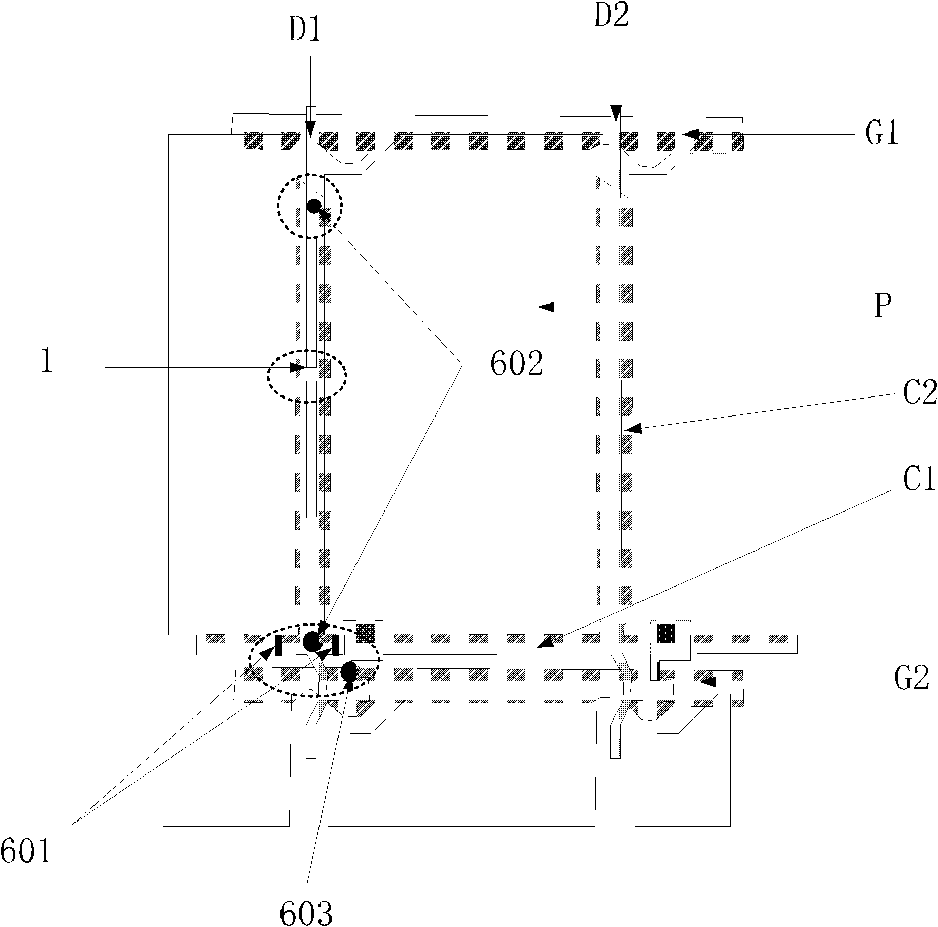
[0041] This embodiment discloses a thin film transistor liquid crystal display device, including:
[0042]substrate, gate line, common line, gate insulating layer, data line, source electrode, drain electrode and pixel electrode, and the common line includes a first common line arranged along a first direction and a first common line arranged along a second direction The second common line, the first common line and the second common line are an integral structure; a cutting mark is arranged on the first common line, and the cutting mark is located on both sides of the second common line and adjacent to the The second common line: the pixel electrode is provided with a cut-off area gap at the position corresponding to the cut-off mark, and the pixel electrode will not be touched during the process of cutting the first common line at the cut-off mark .
[0043] Specific settings such as figure 2 Shown:
[0044] A substrate (not shown in the figure), the substrate is a glass...
Embodiment 2
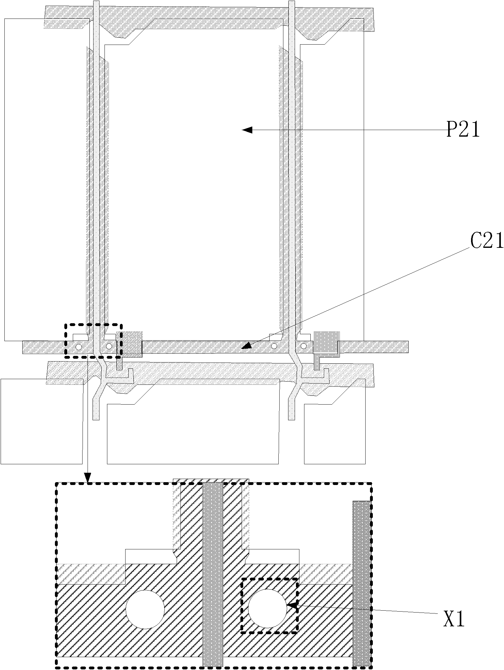
[0058] The difference between this embodiment and the first embodiment is that, if image 3 As shown, a cutting mark X1 is provided on the first common line C21, and the cutting mark X1 has a pattern inside the first common line C21 and passing through the first common line C21, and the pattern In addition, the figure can also be a rectangle, a triangle or other cut-off mark graphics that can play a marking role. It should be noted that the specification of the cut-off mark X1 should be moderate, and it should not be too small to make it difficult for operators to identify , and should not be too large to affect the overall display effect of the liquid crystal display device.
[0059] In the process of repairing the broken data line, when the first common line C21 is cut off, the position to be cut can be accurately judged according to the cut mark X1, and since the pixel electrode is provided with a cut-off region gap, it can be cut at the cut mark. During the process of the...
Embodiment 3
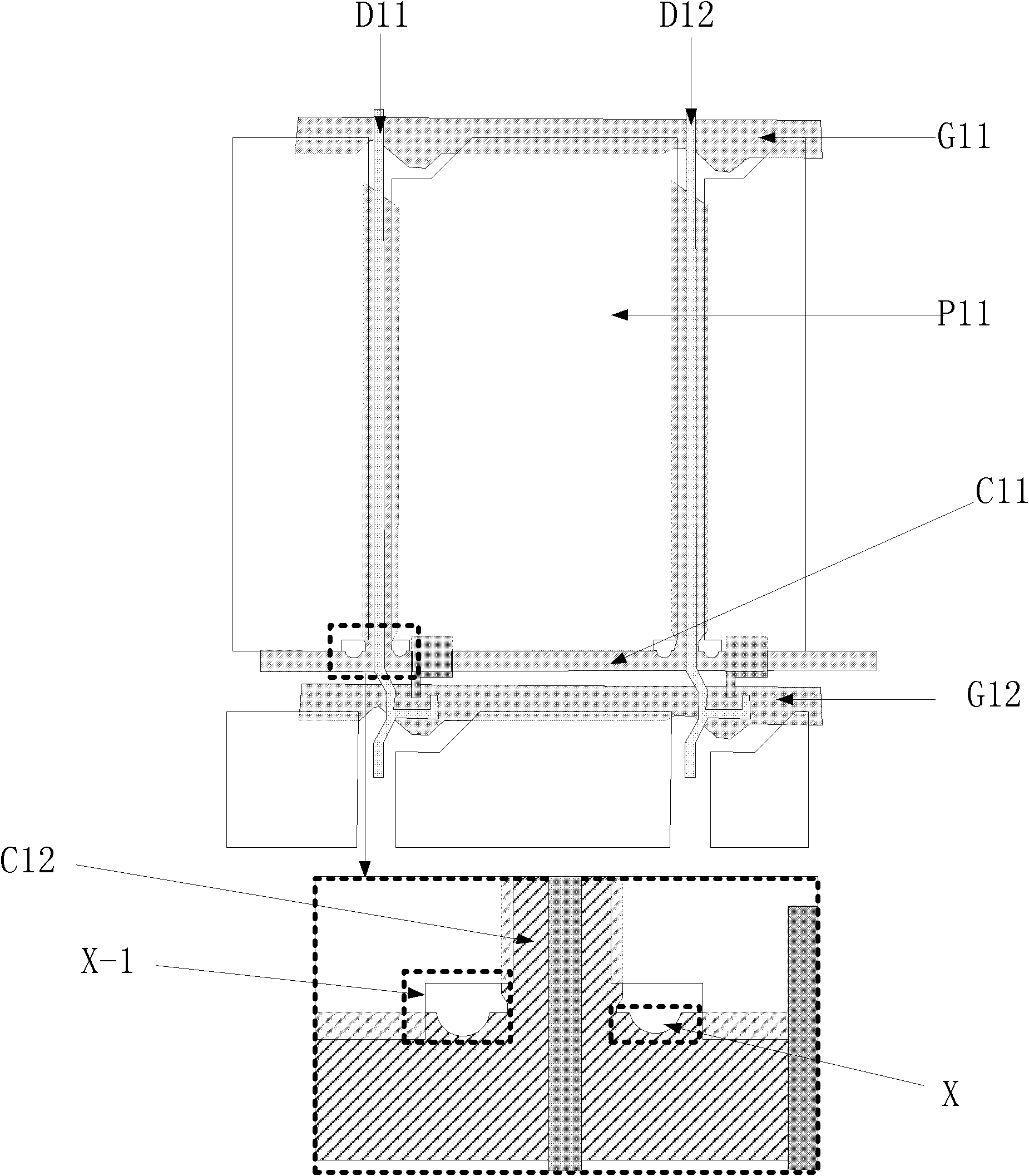
[0061] This embodiment discloses a method for repairing a broken data line of a liquid crystal display device disclosed in Embodiment 1. The method includes:
[0062] Power-on test the liquid crystal display device, determine the broken data line and its corresponding pixel, such as Figure 4 As shown, the broken data line D11-1 is determined, the cutting position 101 marked by the cutting mark X' is laser cut, and the first common line C11-1 is cut off, so that the second common line C12-1 and the second common line C12-1 A common line C11-1 is disconnected, and then the data line D11-1 and the second common line C12-1 are welded together with a laser at the first welding position 102, and at the same time, at the second welding position 103, the disconnected line The data line D11-1 is soldered together with the drain and gate of corresponding pixels.
[0063] So far, a section of the common line has been abandoned, and the pixel corresponding to the broken data line has be...
PUM
 Abstract
Description
Claims
Application Information
 - R&D
- Intellectual Property
- Life Sciences
- Materials
- Tech Scout
- Unparalleled Data Quality
- Higher Quality Content
- 60% Fewer Hallucinations
Browse by: Latest US Patents, China's latest patents, Technical Efficacy Thesaurus, Application Domain, Technology Topic, Popular Technical Reports.
© 2025 PatSnap. All rights reserved.Legal|Privacy policy|Modern Slavery Act Transparency Statement|Sitemap|About US| Contact US: help@patsnap.com