Schottky semiconductor device with insulating layer isolation structure and preparation method thereof

An isolation structure, semiconductor technology, applied in the direction of semiconductor/solid-state device manufacturing, semiconductor devices, electrical components, etc., can solve the problems of multiple times, high on-resistance and reverse leakage current characteristics, and improve the reverse breakdown voltage , Reduce the forward conduction resistance, improve the effect of forward conduction characteristics

Inactive Publication Date: 2013-06-05
朱江 +1
View PDF4 Cites 3 Cited by
  • Summary
  • Abstract
  • Description
  • Claims
  • Application Information

AI Technical Summary

Problems solved by technology

The manufacturing process of the traditional trench Schottky diode requires more masks and manufacturing steps, and the traditional trench Schottky diode has high on-resistance and reverse leakage current characteristics

Method used


Image

  • Schottky semiconductor device with insulating layer isolation structure and preparation method thereof
  • Schottky semiconductor device with insulating layer isolation structure and preparation method thereof
  • Schottky semiconductor device with insulating layer isolation structure and preparation method thereof

Examples


Embodiment 1

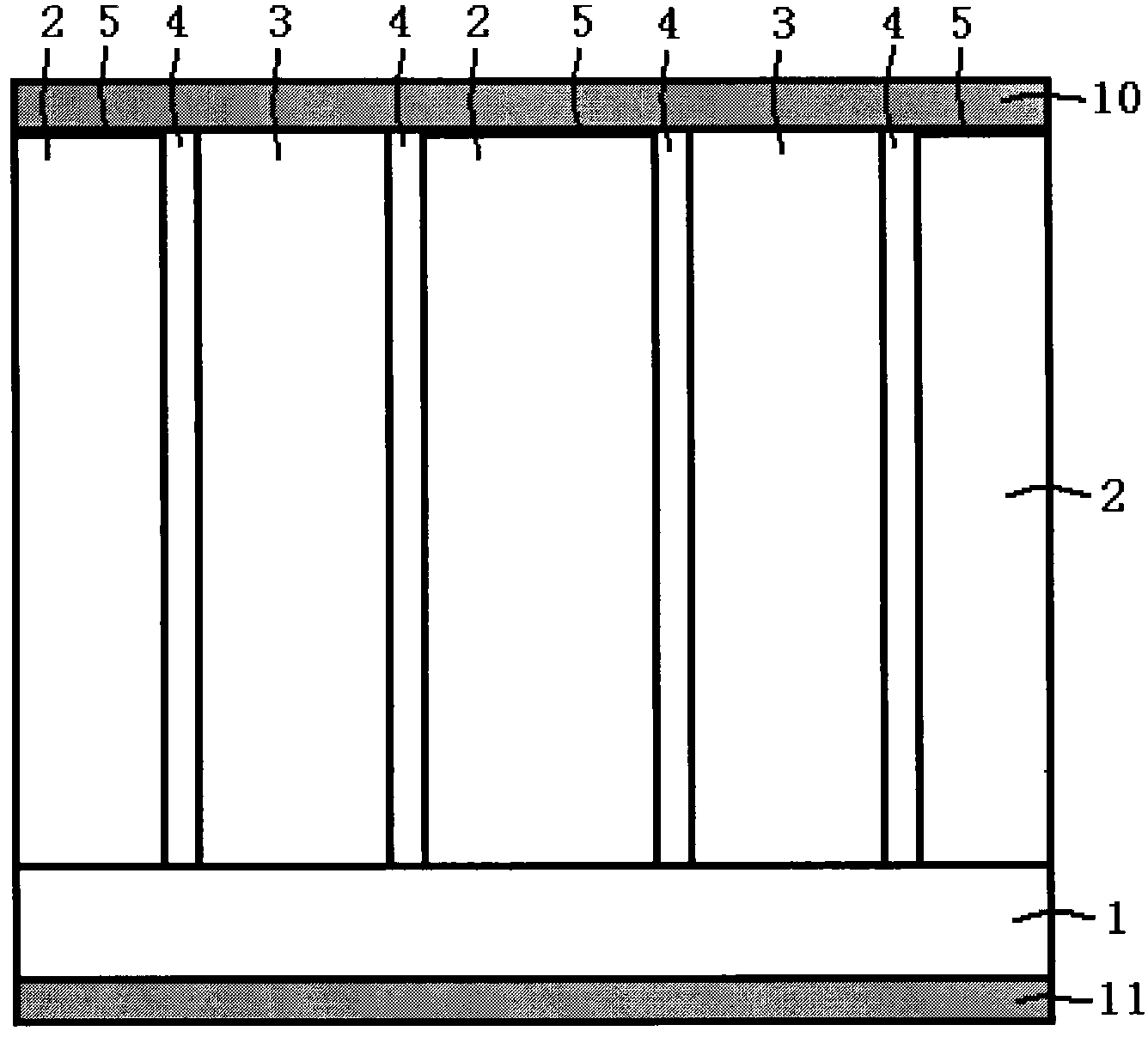
[0033] figure 1 It is a Schottky semiconductor device with an insulating layer isolation structure of the present invention, combined below figure 1 The semiconductor device of the present invention will be described in detail.

[0034] A Schottky semiconductor device with an insulating layer isolation structure, comprising: a substrate layer 1, which is a semiconductor silicon material of N conductivity type, and the doping concentration of phosphorus atoms is 1E19 / CM 3 , on the lower surface of the substrate layer 1, the electrode is drawn out through the lower surface metal layer 11; the N-type semiconductor silicon material 2, located on the substrate layer 1, is an N-conduction type semiconductor silicon material, and the doping concentration of phosphorus atoms is 1E16 / CM 3 ; P-type semiconductor silicon material 3, located on the upper part of the substrate layer 1, is a semiconductor silicon material of P conductivity type, and the doping concentration of boron atoms ...


PUM


Abstract

The invention discloses a Schottky semiconductor device with an insulating layer isolation structure. Through a trench structure, deep strip P-type semiconductor silicon materials 3 can be achieved, and ideal vertical strip semiconductor materials can be achieved through insulating layer isolation. When an apparatus is connected with a reverse bias voltage, the strip P-type semiconductor silicon materials 3 and strip N-type semiconductor silicon materials 2 form charge complementation to form a super-junction structure, and accordingly, the electric field intensity distribution of drift regions is changed, and flat field intensity distribution curves are formed. The invention further provides a preparation method of the Schottky semiconductor device with the insulating layer isolation structure.

Description

technical field [0001] The invention relates to a Schottky semiconductor device with an insulating layer isolation structure, and also relates to a preparation method of the Schottky semiconductor device with an insulating layer isolation structure. Background technique [0002] Power semiconductor devices are widely used in power management and power applications, especially semiconductor devices with trench structures have become an important trend in device development. Schottky devices have the advantages of low forward turn-on voltage and fast turn-on and turn-off speed. Schottky devices also have a large reverse leakage current and cannot be used in high-voltage environments. [0003] Schottky diodes can be fabricated by a number of different layout techniques, the most common being planar layout. A typical trench-type layout is shown in B J Baliga Patent No. 5,612,567. The manufacturing process of the traditional trench Schottky diode requires more masks and manufac...

Claims


Application Information

Patent Timeline
Patent Type & Authority Applications(China)
IPC IPC(8): H01L29/872H01L29/06H01L21/329
Inventor 朱江盛况
Owner 朱江
Why Eureka
Try Eureka