A flexible electronic device, method for manufacturing same, and a flexible substrate

A flexible electronic device and flexible substrate technology, which is applied in semiconductor/solid-state device manufacturing, electric solid-state device, printed circuit manufacturing, etc., can solve the problems of economical reduction, surface roughness reduction, high-temperature processing, etc., and achieve saving Processing time and cost, effect of low cost

Inactive Publication Date: 2013-06-05
POHANG IRON & STEEL CO LTD
View PDF7 Cites 18 Cited by
  • Summary
  • Abstract
  • Description
  • Claims
  • Application Information

AI Technical Summary

Problems solved by technology

However, in the case of using a polymer material to reduce the surface roughness, it cannot be subjected to high temperature processing as in the plastic substrate processing described above.
In addition, the polishing process is suitable for manufacturing high-priced microprocessors or RAMs using a single crystalline silicon (Si) substrate, and is less economical for cheap, large-scale flexible electronics

Method used


Image

  • A flexible electronic device, method for manufacturing same, and a flexible substrate
  • A flexible electronic device, method for manufacturing same, and a flexible substrate
  • A flexible electronic device, method for manufacturing same, and a flexible substrate

Examples


Embodiment 2

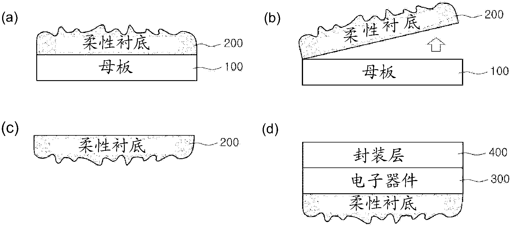
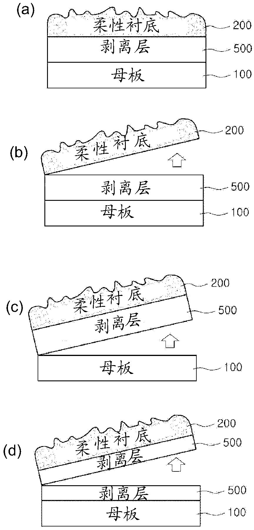
[0082] Such as figure 2 As shown in a, different from Embodiment 1, in Embodiment 2, the flexible substrate 200 is manufactured by forming a release layer 500 between the motherboard 100 and the flexible substrate 200 . When the peeling layer 500 is formed, the separation form of the flexible substrate 200 can be as follows: it can be separated from the interface of the flexible substrate 200 ( figure 2 b), or separated from the interface between the motherboard 100 and the release layer 500 ( figure 2 c), or separated from the inner surface of the release layer 500 ( figure 2 d). at this time, figure 2 The case of b does not require subsequent processing, but figure 2 c and figure 2 The case of d may also include removing the peeling layer 500 .

[0083] In Example 2 of the present invention, an ITO layer as a peeling layer is formed on a glass substrate with a thickness of 120 nm, and a Ti / Au / Cu flexible substrate is formed by forming a 50 nm layer for forming a...

Embodiment 3

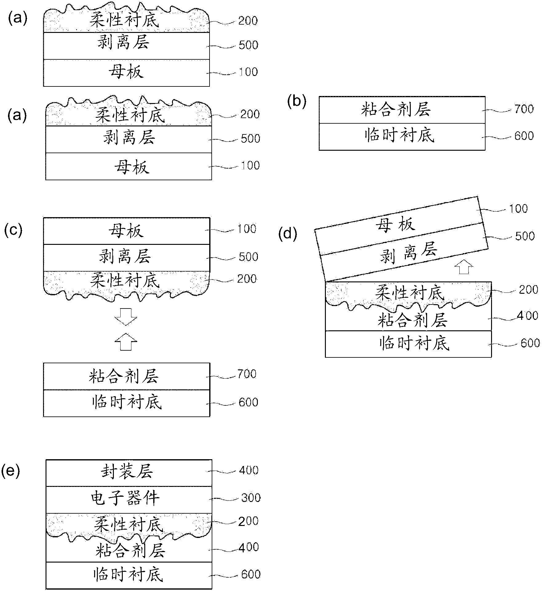
[0085] image 3 A method of manufacturing a flexible electronic device according to a third embodiment of the present invention is schematically shown. Such as image 3 As shown, in the method for manufacturing a flexible electronic device according to the third embodiment of the present invention, a flexible substrate 200 is formed on a motherboard 100, wherein a release layer 500 is placed between the motherboard 100 and the flexible substrate 200 ( image 3 a), bonding the temporary substrate 600 on the flexible substrate 200, wherein the adhesive layer 700 is placed between the flexible substrate 200 and the temporary substrate 600 ( image 3 c). After that, the motherboard 100 formed on the flexible substrate 200 is separated by the peeling layer 500 ( image 3 d), forming an electronic device 300 and an encapsulation layer 400 on the separated surface of the flexible substrate 200 to manufacture a flexible electronic device ( image 3 e).

[0086] That is, the metho...


PUM

PropertyMeasurementUnit
thicknessaaaaaaaaaa
thicknessaaaaaaaaaa
thicknessaaaaaaaaaa

Abstract

The present invention relates to resolving the issues concerning the deterioration in the performance and yield of a flexible electronic device, which are caused by low manufacturing temperature, high surface roughness, a high thermal expansion coefficient, and the bad handling characteristics of a typical flexible substrate. The method for manufacturing a flexible electronic device according to the present invention includes: forming a flexible substrate on a motherboard while physically separating the interface therebetween so that the interfacial bonding therebetween has a yield strength less than that of the flexible substrate; and forming an electronic device on the separated surface of the flexible substrate which had previously been in contact with the motherboard.

Description

technical field [0001] The present invention relates to a flexible electronic device (Flexible Electronic Device) and a method for manufacturing the flexible electronic device, as well as a flexible substrate used in the flexible electronic device, more particularly, to a method for manufacturing a flexible electronic device comprising the following flexible substrate The method for electronic devices, the flexible substrate has low surface roughness and low thermal expansion coefficient, can be used for high temperature glass substrate processing, and has a new structure with excellent operating characteristics. Background technique [0002] Currently, with the development of information technology (IT), the importance of flexible electronic devices is increasing. Therefore, organic light emitting displays (organic light emitting display: OLED), liquid crystal displays (liquid crystal display: LCD), electrophoretic displays (Electrophoretic display: EPD), and plasma display...

Claims


Application Information

Patent Timeline
Patent Type & Authority Applications(China)
IPC IPC(8): H01L51/56H01L51/52
CPCH01L51/003B32B7/12H01L29/78603B32B27/36H01L2251/5338H01L51/56H05K1/0277H01L51/0097H05K3/303H01L27/1266H01L51/52H01L27/1218H01L2227/326Y02E10/549Y10T29/4913Y02P70/50H10K71/80H10K77/111H10K50/80H10K59/1201H10K71/00H10K2102/311
Inventor 李钟览金基洙
Owner POHANG IRON & STEEL CO LTD
Why Eureka
Try Eureka