Printed circuit board assembly (PCBA) board testing system and PCBA board testing method

A test system and test method technology, applied in the direction of electronic circuit test, etc., can solve the problems of high management cost and low test efficiency of PCBA board, and achieve the effect of improving efficiency, improving test efficiency and reducing test cost

Active Publication Date: 2013-06-12
SUZHOU INOVANCE TECH CO LTD
View PDF8 Cites 25 Cited by
  • Summary
  • Abstract
  • Description
  • Claims
  • Application Information

AI Technical Summary

Problems solved by technology

[0006] The technical problem to be solved by the present invention is to provide a PCBA board testing system

Method used


Image

  • Printed circuit board assembly (PCBA) board testing system and PCBA board testing method
  • Printed circuit board assembly (PCBA) board testing system and PCBA board testing method
  • Printed circuit board assembly (PCBA) board testing system and PCBA board testing method

Examples


Embodiment Construction

[0029] In order to make the object, technical solution and advantages of the present invention clearer, the present invention will be further described in detail below in conjunction with the accompanying drawings and embodiments. It should be understood that the specific embodiments described here are only used to explain the present invention, not to limit the present invention.

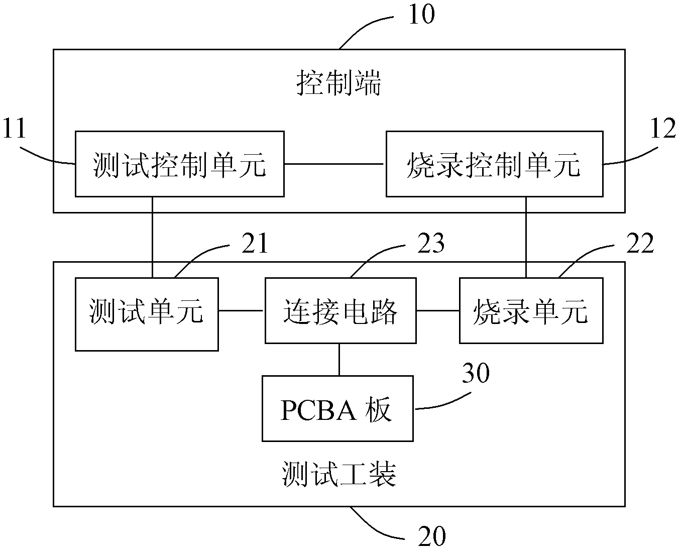
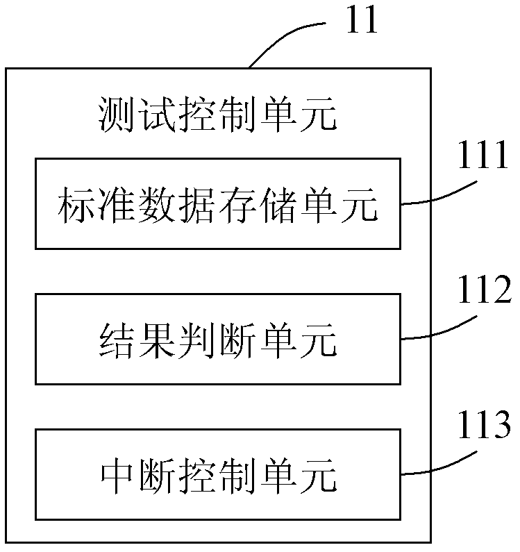
[0030] Such as figure 1 Shown is a schematic diagram of a PCBA board testing system embodiment of the present invention. In this embodiment, the PCBA board 30 to be tested includes multiple functional circuits and at least one programmable chip, and the testing system includes a control terminal 10 and at least one testing tool 20 . The test tooling 20 includes a test unit 21 , a programming unit 22 and a connection circuit 23 . The control terminal 10 includes a test control unit 11 and a programming control unit 12 . The testing unit 21 and the programming unit 22 are respectively connected to...


PUM


Abstract

The invention provides a printed circuit board assembly (PCBA) board testing system. The PCBA board testing system comprises a control end and a testing tool. The testing tool comprises a testing unit, a burn unit and a connecting circuit, wherein the connecting circuit is connected with a testing pin and a burn pin of a PCBA board. The control end comprises a burn control unit and a testing control unit, the burn control unit is used for controlling the burn unit to carry out program burn on a programmable chip on the PCBA board. The testing control unit is used for controlling the testing unit to carry out testing on each function circuit of the PCBA board, calling the burn control unit to carry out burn control, and carrying out testing on the burnt programmable chip and a chip control circuit of the PCBA board. The invention further provides a PCBA board testing method. According to the PCBA board testing system and the PCBA board testing method, due to the fact that a burn program is inlaid into an automatic testing process, a function circuit testing process and a burn process are simultaneously carried out, not only is the testing tool saved, but also efficiency is improved.

Description

technical field [0001] The invention relates to the field of chip programming and testing, and more specifically, to a PCBA board testing system and method. Background technique [0002] With the rapid development of electronic industry automation, a large number of various programmable chips were born. Thus, various IC programming (burning) devices have been produced. [0003] The existing burning method is as follows: manually place the programmable chip to be burned on the program burner, and burn the program into the programmable chip; Go to the PCBA board and then conduct the overall test of the PCBA board. [0004] However, the use of the above-mentioned burning equipment is too single, and the cost is high; and the method of using the burning software to burn through the burner is complicated to operate, and operation errors are prone to occur during the burning process, resulting in an increase in the defective rate of the product; in addition, The above-mentioned...

Claims


Application Information

Patent Timeline
IPC IPC(8): G01R31/28
Inventor 王宗超
Owner SUZHOU INOVANCE TECH CO LTD
Why Eureka
Try Eureka