Pixel compensation circuit for AMOLED (Active Matrix/Organic Light Emitting Diode) displayer

A technology for compensating circuits and displays, applied in static indicators, instruments, etc., can solve problems such as drift, poor display quality, uneven brightness, etc., achieve stable current output, eliminate the dependence of threshold threshold voltage, and maintain current output Effect

Inactive Publication Date: 2013-06-12
AU OPTRONICS CORP
View PDF0 Cites 71 Cited by
  • Summary
  • Abstract
  • Description
  • Claims
  • Application Information

AI Technical Summary

Problems solved by technology

However, in the driving mechanism of AMOLED display, OLED controls the brightness of light emission based on the magnitude of the current flowing through it, and the electrical parameters of the thin film transistor used for driving will directly affect the display effect of the screen
For example, due to the influence of the manufacturing process, the threshold voltage (threshold voltage) of the thin film transistor in each pixel may drift. At this time, even if the

Method used


Image

  • Pixel compensation circuit for AMOLED (Active Matrix/Organic Light Emitting Diode) displayer
  • Pixel compensation circuit for AMOLED (Active Matrix/Organic Light Emitting Diode) displayer
  • Pixel compensation circuit for AMOLED (Active Matrix/Organic Light Emitting Diode) displayer

Examples


Embodiment Construction

[0038] In order to make the technical content disclosed in this application more detailed and complete, reference may be made to the drawings and the following various specific embodiments of the present invention, and the same symbols in the drawings represent the same or similar components. However, those skilled in the art should understand that the examples provided below are not intended to limit the scope of the present invention. In addition, the drawings are only for schematic illustration and are not drawn according to their original scale.

[0039] The specific implementation manners of various aspects of the present invention will be further described in detail below with reference to the accompanying drawings.

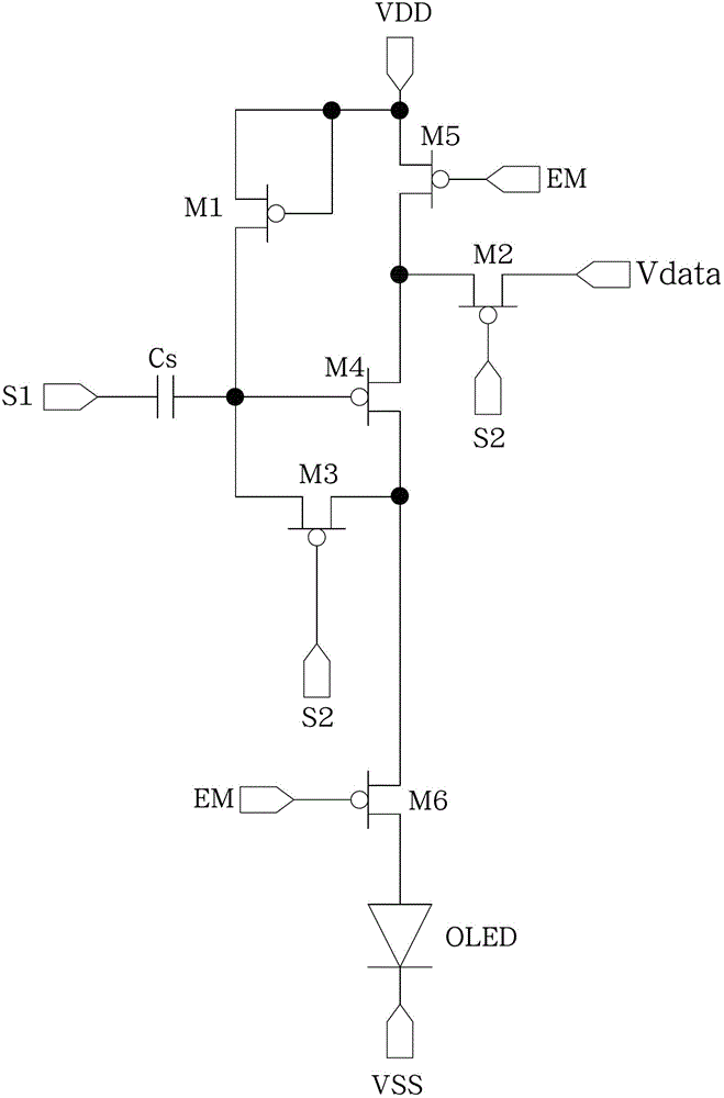
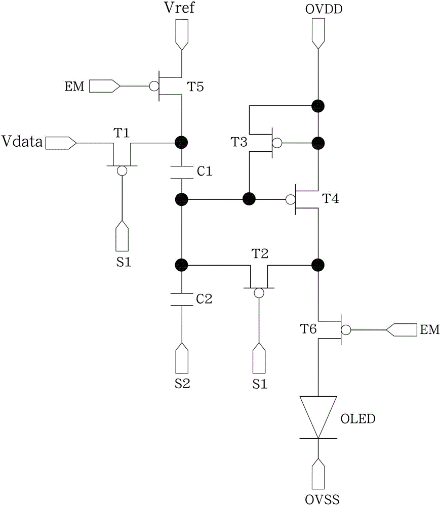
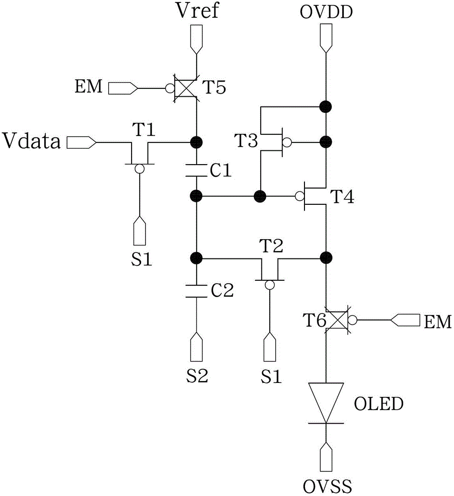
[0040] figure 1 A schematic diagram showing the principle of a pixel compensation circuit for an AMOLED display using a 6T1C architecture in the prior art, figure 2 show figure 1 Schematic diagram of the timing of key signals of the pixel compensation c...


PUM


Abstract

The invention provides a pixel compensation circuit. The pixel compensation circuit comprises a first switch, a second switch, a third switch, a fourth switch, a fifth switch, a sixth switch, a first capacitor, a second capacitor and an organic light-emitting diode, wherein a first end of the first switch receives data voltage; a second end of the first switch receives a first switch signal; a second end of the second switch receives the first switch signal; a second end and a third end of the third switch are both connected to first voltage; a first end of the fifth switch receives reference voltage; a second end of the fifth switch receives a third switch signal; a second end of the sixth switch receives the third switch signal; a first end of the second capacitor is connected to a second end of the first capacitor; a second end of the second capacitor receives a second switch signal; a first end of the organic light-emitting diode is connected to a first end of the sixth switch; and a second end of the organic light-emitting diode is connected to second voltage. Compared with the prior art, the pixel compensation circuit has the advantages that the threshold value voltage of the switches is compensated before a lightening period, so that the influence of the threshold vale voltage on OLED (Organic Light Emitting Diode) current is eliminated, and stable current output of an OLED in a pixel can be kept.

Description

technical field [0001] The invention relates to an active matrix organic light emitting diode display, in particular to a pixel compensation circuit of the AMOLED display. Background technique [0002] Organic light emitting diodes (Organic Light Emitting Diode, OLED) can be divided into passive matrix driving (Passive Matrix OLED, PMOLED) and active matrix driving (Active Matrix OLED, AMOLED) according to the driving method. Among them, the PMOLED does not emit light when data is not written, but only emits light during data writing. This driving method is simple in structure, low in cost, and easy to design, and is mainly suitable for small and medium-sized displays. [0003] The biggest difference between AMOLED and PMOLED is that each pixel has a capacitor to store data, so that each pixel can maintain a light-emitting state. Since the power consumption of AMOLED is significantly lower than that of PMOLED, and its driving method is suitable for the development of large...

Claims


Application Information

Patent Timeline
IPC IPC(8): G09G3/32G09G3/3233
Inventor 郑士嵩
Owner AU OPTRONICS CORP
Why Eureka
Try Eureka