Photovoltaic module, and processing device and processing technology of photovoltaic module

A technology for photovoltaic modules and processing devices, applied in photovoltaic power generation, sustainable manufacturing/processing, electrical components, etc., can solve problems such as efficiency attenuation, and achieve the effect of eliminating the impact of efficiency deterioration, strong operability, and simple transformation

Pending Publication Date: 2021-11-16
南京和洪智能设备有限公司
View PDF0 Cites 0 Cited by
  • Summary
  • Abstract
  • Description
  • Claims
  • Application Information

AI Technical Summary

Problems solved by technology

[0005] In order to solve the above problems, the present invention provides a device for solving the high temperature dark state attenuation of photovoltaic modules and a processing technology for photovoltaic modules, which involves a simple and efficient solution to solve the problems caused by the module lamination process and other high temperature dark state conditions. The efficiency attenuation problem of
By introducing a specific device, it can eliminate the influence of high-temperature dark state on the deterioration of the efficiency of heterojunction cells, ensure the conversion efficiency of solar cells to the maximum extent, and also have the function of improving the conversion efficiency of solar cells, and solve the problems caused by welding and lamination. The high temperature will cause degradation of solar cell passivation effect and conversion efficiency, thereby increasing the output power of solar cell components. Compared with other methods, this method can be realized on existing equipment, with high compatibility and high cell efficiency. , less energy consumption and other advantages

Method used


Image

  • Photovoltaic module, and processing device and processing technology of photovoltaic module
  • Photovoltaic module, and processing device and processing technology of photovoltaic module
  • Photovoltaic module, and processing device and processing technology of photovoltaic module

Examples


Embodiment 1

[0040] This embodiment relates to a method for processing a photovoltaic module, comprising the following steps:

[0041] 1) First prepare heterojunction solar cells

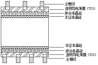
[0042] Using 166-size N-type monocrystalline silicon wafers as substrates, prepare back-emitting heterojunction solar cells. The front side is n-type, and the back side is p-type. Oxide (TCO) layer, N-type amorphous silicon layer (n-Si: H), intrinsic amorphous silicon layer (i-Si: H), N-type crystalline silicon (c-Si), intrinsic amorphous silicon layer (i-Si:H), P-type amorphous silicon layer (p-Si:H), transparent conductive oxide (TCO) layer, back metal grid electrode, battery structure see figure 1 . The obtained silicon heterojunction solar cell is subjected to light injection treatment, and this step can improve the conversion efficiency of the cell sheet.

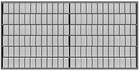
[0043] 2) Connect silicon heterojunction solar cells in series and parallel to form silicon heterojunction solar cell strings: cut the heterojunction...

Embodiment 2

[0050] This embodiment relates to a method for processing a photovoltaic module. The difference between this embodiment and Embodiment 1 is that in step 1), the heterojunction solar cells are not subjected to light injection treatment. According to this process, 5 components were processed, and the power data of the obtained components were measured. The experimentally measured data are shown in Table 1.

Embodiment 3

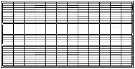
[0052] The difference between this embodiment and embodiment 1 is that in step 2), the heterojunction solar cells are not sliced, and the whole cell is connected in series, and the shape of the components is as follows: image 3 shown. According to this process, 5 components were processed, and the power data of the obtained components were measured. The experimentally measured data are shown in Table 1.


PUM

PropertyMeasurementUnit
thicknessaaaaaaaaaa
thicknessaaaaaaaaaa

Abstract

The invention discloses a photovoltaic module and a processing device and processing technology thereof, and the processing device comprises a power supply device which is used for outputting a direct current and is provided with at least one group of positive and negative electrodes; at least two conductive wires which are used for connecting a power supply device and a to-be-processed component, wherein each conductive wire is connected with the positive electrode and the negative electrode respectively; and a temperature sensing control module which is used for detecting the temperature of the to-be-processed component and the temperature of the power supply device and comparing the detected temperature with a set temperature so as to adjust the current of the power supply device. Through the processing device, the photovoltaic module can be subjected to electric injection in the lamination process, and the current of the power supply device is adjusted by detecting the temperature in the lamination process, so the attenuation problem in the lamination process can be effectively solved, and the attenuation problem in the cooling period after the photovoltaic module is laminated is also solved; and the influence of a high-temperature dark state on the efficiency deterioration of the heterojunction cell is eliminated.

Description

technical field [0001] The invention relates to the field of photovoltaic modules, in particular to a photovoltaic module, a processing device and a processing technology for the photovoltaic module. Background technique [0002] For HJT cells, amorphous silicon plays a key role in passivation and the formation of p-n junctions, and plays a decisive role in the conversion efficiency of HJT cells. Therefore, the preparation of amorphous silicon thin films with excellent performance is the key technology for obtaining high-efficiency HJT cells. In previous studies, hydrogenated amorphous silicon (a-Si:H) undergoes light-induced attenuation due to the so-called Staebler-Wronski effect (Staebler-Wronski effect), which is considered to be related to the fact that the a-Si network contains a large number of free Hydrogen is closely related. In silicon heterojunction solar cells, since the amorphous silicon layer contains a large number of hydrogen bonds and silicon dangling bonds...

Claims


Application Information

Patent Timeline
Patent Type & Authority Applications(China)
IPC IPC(8): H01L31/20H01L21/67B32B38/00
CPCH01L31/202H01L21/67253B32B38/0008Y02E10/50Y02P70/50
Inventor 张巧华
Owner 南京和洪智能设备有限公司
Why Eureka
Try Eureka