
Light-emitting diode (LED) power source with inversed LED chip and method for producing LED power source with inversed LED chip

A technology of LED chip and LED light source, which is applied in the direction of electrical components, electrical solid devices, circuits, etc., can solve the problems of insignificant improvement of reflective effect and low light transmittance, reduce the complexity of the preparation process, improve the light extraction efficiency, The effect of consistency guarantee

Inactive Publication Date: 2013-06-12
ELEC TECH OPTOELECTRONICS TECHWUHUCO
View PDF6 Cites 4 Cited by
  • Summary
  • Abstract
  • Description
  • Claims
  • Application Information

AI Technical Summary

Problems solved by technology

For the structure of NiO / Au-based multilayer film plus Ag film or Al film with high reflectivity, most of the reflected light is also absorbed due to the low light transmittance of NiO / Au-based multilayer film, making it reflective. The increase is also not obvious

Method used

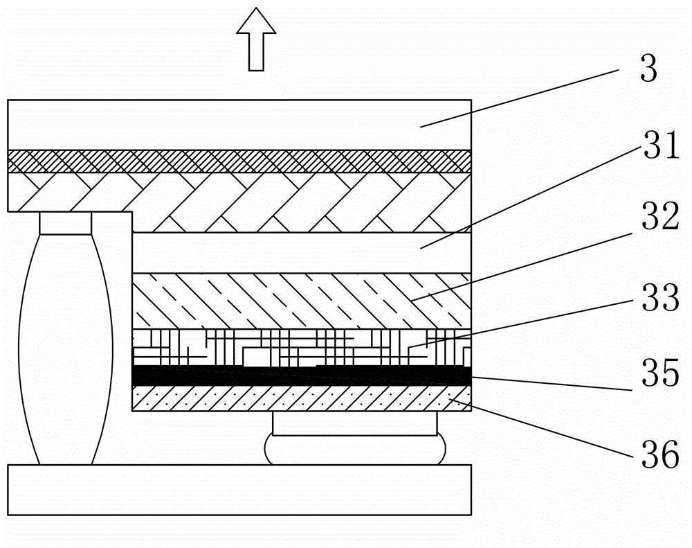

Image

  • Light-emitting diode (LED) power source with inversed LED chip and method for producing LED power source with inversed LED chip
  • Light-emitting diode (LED) power source with inversed LED chip and method for producing LED power source with inversed LED chip
  • Light-emitting diode (LED) power source with inversed LED chip and method for producing LED power source with inversed LED chip

Examples


Embodiment Construction

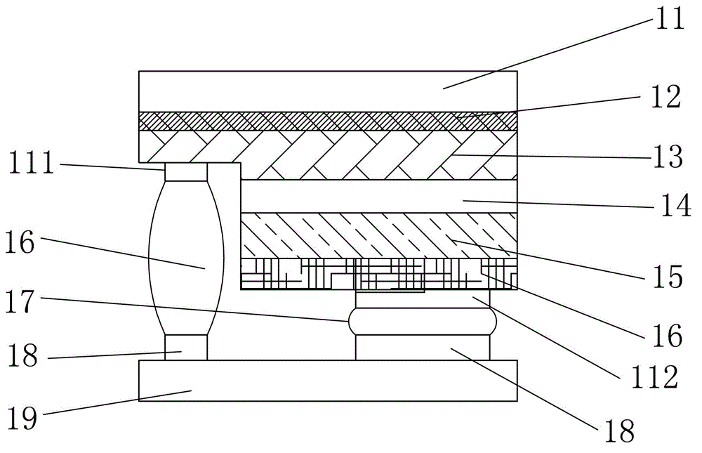
[0039] see image 3 , the LED light source described in the figure includes an LED chip and a substrate 19; the LED chip includes a transparent substrate 11, an N-type cladding layer 13, an active layer 14, a P-type cladding layer 15, a transparent Conductive film layer 16. Wherein, the active layer 14 is a single layer or MQW layer structure.

[0040] An N-type electrode plate 111 is provided on the exposed area of ​​the N-type cladding layer 13, and a metal bump 16 is provided on the N-type electrode plate 111; a P-type electrode plate is provided on the transparent conductive film layer 16. An electrode pad 112 , the P-type electrode pad 112 is provided with metal bumps 17 .

[0041] The substrate 19 is a transparent substrate, on which a metal boss 18 and positive and negative electrodes (not shown) for connecting to an external circuit are provided; the metal bump on the N-type electrode plate 111 16 and the metal bumps 17 on the P-type electrode plate 112 are connecte...


PUM


Abstract

The invention discloses a light-emitting diode (LED) power source with an inversed LED chip and a method for producing the LED power source with the inversed LED chip. The LED power source with the inversed LED chip provided by the invention comprises the LED chip and a base plate, wherein the LED chip comprises a transparent substrate, an N-type coating, an active layer, a P-type coating and a transparent conducting thin film which are sequentially superposed together; an N-type electrode pad is arranged in an exposed area of the N-type coating, and a metal salient point is arranged on the N-type electrode pad; a P-type electrode pad is arranged on the transparent conducting thin film, and a metal salient point is arranged on the P-type electrode pad; the base plate is a transparent base plate, and metal bosses, and a positive electrode and a negative electrode which are used for being connected with an external circuit are arranged on the base plate; and the metal salient points on the N-type electrode pad and the P-type electrode pad are respectively and correspondingly connected with the metal bosses on the base plate, and an encapsulation glue is also arranged on the base plate and covers the LED chip. The light-emitting efficiency of the chip is increased, the chip structure is simplified, and the production technological complexity of the chip is lowered.

Description

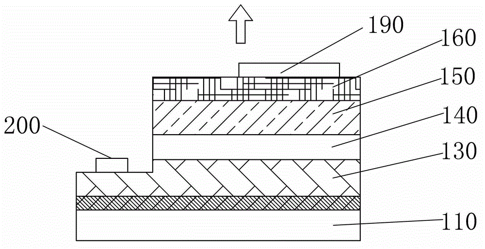
technical field [0001] The invention relates to the technical field of LEDs, in particular to an LED light source with flip-chip LED chips and a manufacturing method thereof. Background technique [0002] Gallium nitride-based LED chips have been widely used in many fields such as lighting, indication, display and backlight. For LED chips prepared using sapphire substrates, since sapphire is a non-conductive insulator, the positive and negative electrodes of the LED chip must be prepared on the same side of the chip. see figure 1 , the conventional front-mount LED chip structure is to grow gallium nitride-based quantum well 140 semiconductor material on sapphire substrate 110 . The N-type GaN layer 130 is etched to form an exposed area. Then, a transparent conductive film 160 is formed on the P-type GaN layer 150 as a current spreading layer and a light-transmitting layer. [0003] For the GaN-based LED chip, the transparent conductive film 160 is made of Ni / Au material....

Claims


Application Information

Patent Timeline
Patent Type & Authority Applications(China)
IPC IPC(8): H01L33/48
CPCH01L24/97H01L2224/14H01L2224/16225H01L2924/12041H01L2924/00
Inventor 王冬雷
Owner ELEC TECH OPTOELECTRONICS TECHWUHUCO
Learn More