Ultra-high-speed aes processor based on fpga and its realization method

An implementation method and processor technology, applied in the field of communications, can solve problems such as large resource occupation, long delay time, complex control logic, etc., and achieve the effects of ensuring effectiveness, improving reliability, and simple storage control logic.

Inactive Publication Date: 2016-01-20
XIDIAN UNIV
View PDF4 Cites 0 Cited by
  • Summary
  • Abstract
  • Description
  • Claims
  • Application Information

AI Technical Summary

Problems solved by technology

[0006] The purpose of the present invention is to overcome the deficiencies of the above-mentioned prior art, solve the problems of traditional AES processor control logic complexity, long delay time between input and output, and occupy more resources, and propose a method with faster calculation speed and resource utilization FPGA-based ultra-high-speed AES processor with higher rate and simpler structure and its implementation method to improve its practical performance

Method used


Image

  • Ultra-high-speed aes processor based on fpga and its realization method
  • Ultra-high-speed aes processor based on fpga and its realization method
  • Ultra-high-speed aes processor based on fpga and its realization method

Examples


Embodiment Construction

[0042] The present invention will be further described below in conjunction with the drawings.

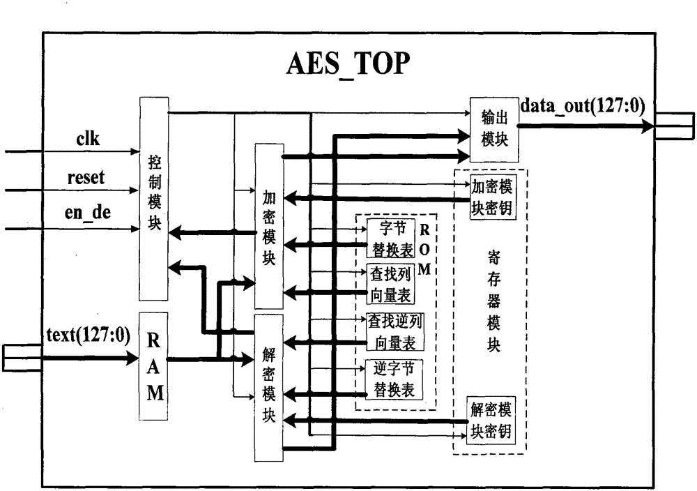
[0043] Reference attached figure 1 The overall structure of the processor of the present invention will be further described.

[0044] The processor of the present invention includes an interface storage area buffer module, a control module, an AES encryption and decryption module, a read-only memory look-up table module, a register module, and an output module; the interface storage area buffer module and the AES encryption and decryption module are connected to the control bus through a data bus ; Read-only memory look-up table module, register module, control module, output module are connected with the control bus through the data bus.

[0045] The interface storage area buffer module is used to temporarily store the data on the input data bus. The interface storage area buffer module includes four random access memory RAMs arranged in the front buffer of the encryption and decryptio...


PUM


Abstract

The invention discloses a field programmable gate array (FPGA)-based superfast auxiliary encoder system (AES) processor and an implementing method thereof. The AES processor comprises an interface storage area buffer module, a control module, an AES encryption and decryption module, a read-only memory lookup table module, a register module and an output module. The implementing method for the processor comprises the following steps: 1, initializing a data table; 2, performing initial setting; 3, receiving data; 4, reading the data; 5, selecting a data processing mode; 6, judging whether the encryption and decryption are finished; and 7, outputting a result. The invention mainly solves the problems that an AES processor is controlled complicatedly and modules have low portability, reliability, safety and processing speed in the prior art; and an improved algorithm and a lookup table-based method are used. The AES processor has all levels of structures which are fixed, is simple in control logic, comprises the modules with high portability, is suitable to be implemented in a singlechip FPGA, and has the characteristics of high speed and high accuracy.

Description

Technical field [0001] The invention belongs to the field of communication technology, and further relates to a field programmable gate array (Field Programmable Gate Array, FPGA)-based ultra-high-speed Advanced Encryption Standard (AES) processor and its implementation method in the field of information security technology. The invention fully utilizes the flexibility of FPGA programming and the reliability of hardware under the condition of ensuring high processing speed and minimum resource occupation, and realizes the safe encryption of data and information. The invention can be widely applied to advanced encryption and decryption in smart cards, mobile banking systems, and ATM cash machines to ensure the safety of data and information. Background technique [0002] With the development of communication technology, the communication environment has become increasingly complex. Compared with traditional software encryption methods, hardware encryption has the advantages of fas...

Claims


Application Information

Patent Timeline
Patent Type & Authority Patents(China)
IPC IPC(8): H04L9/06
Inventor 刘景伟蔡鑫孙蓉李勇白宝明
Owner XIDIAN UNIV
Why Eureka
Try Eureka