Eureka AIR delivers breakthrough ideas for toughest innovation challenges, trusted by R&D personnel around the world.

Monitoring method of millisecond annealing process stability

A millisecond annealing and stability technology, applied in measuring devices, measuring electrical variables, measuring resistance/reactance/impedance, etc., can solve the problems of low millisecond annealing process accuracy, unreusable wafers to be monitored, and increased production costs. , to achieve the effect of high accuracy, convenient compensation and improved efficiency

Active Publication Date: 2015-11-25
SEMICON MFG INT (SHANGHAI) CORP
View PDF7 Cites 0 Cited by
  • Summary
  • Abstract
  • Description
  • Claims
  • Application Information

AI Technical Summary

Problems solved by technology

[0006] The stability monitoring method of the existing rapid thermal annealing process, the wafer to be monitored cannot be reused, which increases the production cost, and the existing monitoring method is less accurate in monitoring the stability of the millisecond annealing process

Method used


Image

  • Monitoring method of millisecond annealing process stability
  • Monitoring method of millisecond annealing process stability
  • Monitoring method of millisecond annealing process stability

Examples


Embodiment Construction

[0034] In the process of monitoring the stability of the rapid thermal annealing process, the inventor found that after the ion implantation of the wafer to be monitored, due to the difference in the thickness of the wafer and the depth of ion implantation, the implanted area cannot be removed by etching The silicon material realizes the repeated utilization of the monitoring wafer, which increases the production cost.

[0035] The inventors have further studied and found that when the existing monitoring method for the stability of the rapid thermal annealing process monitors the stability of the millisecond annealing process, the sheet resistance value on the monitoring wafer and the temperature of the millisecond annealing process are non-linear changes, making the monitoring The error increases, and the accuracy of monitoring is low, especially for low temperature areas, this effect is particularly serious.

[0036] In order to solve the above problems, the inventor propos...


PUM

PropertyMeasurementUnit
thicknessaaaaaaaaaa
thicknessaaaaaaaaaa
thicknessaaaaaaaaaa

Abstract

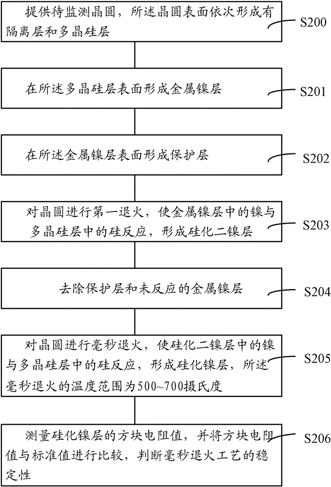
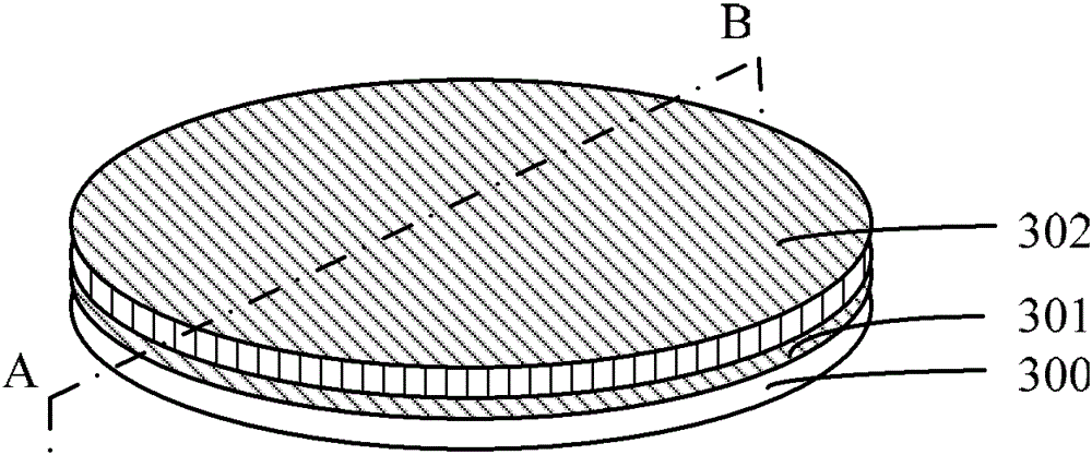
The invention provides a monitoring method of millisecond annealing process stability. The method includes that to-be-monitored wafers are provided, isolated layers and polycrystalline silicon layers are formed on the surfaces of the wafers in sequence; metal nickel layers are formed on the surfaces of the polycrystalline silicon layers; a first annealing is conducted to the waders, nickel of the metal nickel layers reacts with silicon of the polycrystalline silicon layers to form silicification double nickel layers; the metal nickel layers which are not reacted are eliminated; millisecond annealing are conducted to the wafers, the nickel of the silicification double nickel layers reacts with the silicon of the polycrystalline silicon layers to form silicification nickel layers, and the temperature range of the millisecond annealing is 500 DEG C-700DEG C; square resistance values of the silicification nickel layers are measured, the square resistance values are compared with standard values to judge the millisecond annealing process stability. The monitoring method of the millisecond annealing process stability improves using ratio of monitoring the wafers, reduces production cost and improves monitoring accuracy.

Description

technical field [0001] The invention relates to the field of semiconductor manufacturing, in particular to a method for monitoring the stability of a millisecond annealing process. Background technique [0002] In the integrated circuit manufacturing process, semiconductor devices are formed on the semiconductor substrate through a series of deposition, photolithography, etching, and planarization processes. With the rapid development of Ultra Large Scale Integration (ULSI), the integrated circuit manufacturing process It is becoming more and more complex and fine, which requires the formation of semiconductor devices with higher precision and better uniformity. During the fabrication of integrated circuits, any fluctuation of process parameters may lead to the failure of the formed semiconductor device, so it becomes very important to monitor the stability of each process of forming the semiconductor device. [0003] The rapid thermal annealing process is a very important ...

Claims


Application Information

Patent Timeline
Patent Type & Authority Patents(China)
IPC IPC(8): H01L21/66G01R27/02
Inventor 何永根禹国宾吴兵
Owner SEMICON MFG INT (SHANGHAI) CORP
Why Eureka
Eureka Blog
Learn More