Printed circuit board

A printed circuit board and board body technology, applied in the direction of printed circuit, printed circuit, printed circuit components, etc., can solve the problems of poor anti-electromagnetic interference ability of printed circuit board 100, unfavorable interference current derivation, high grounding impedance, etc., to achieve improved Anti-electromagnetic interference ability, reduce production cost, and reduce the effect of grounding impedance

Inactive Publication Date: 2013-06-19
HONG FU JIN PRECISION IND (SHENZHEN) CO LTD +1
View PDF2 Cites 12 Cited by
  • Summary
  • Abstract
  • Description
  • Claims
  • Application Information

AI Technical Summary

Problems solved by technology

However, the grounding impedance of the screw 17 is generally high, and the conductive member 16 is easily oxidized by air due to being disposed on the surface of the printed circuit board 100, thereby reducing conductivity.
In this way, it is not conducive to deriving the interference current on the printed circuit board 100, so that the anti-electromagnetic interference capability of the printed circuit board 100 is relatively poor.

Method used


Image

  • Printed circuit board
  • Printed circuit board
  • Printed circuit board

Examples


Embodiment Construction

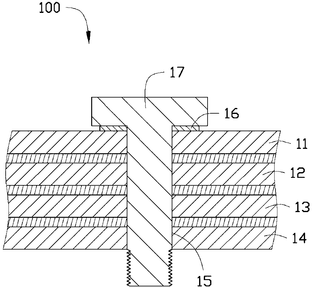
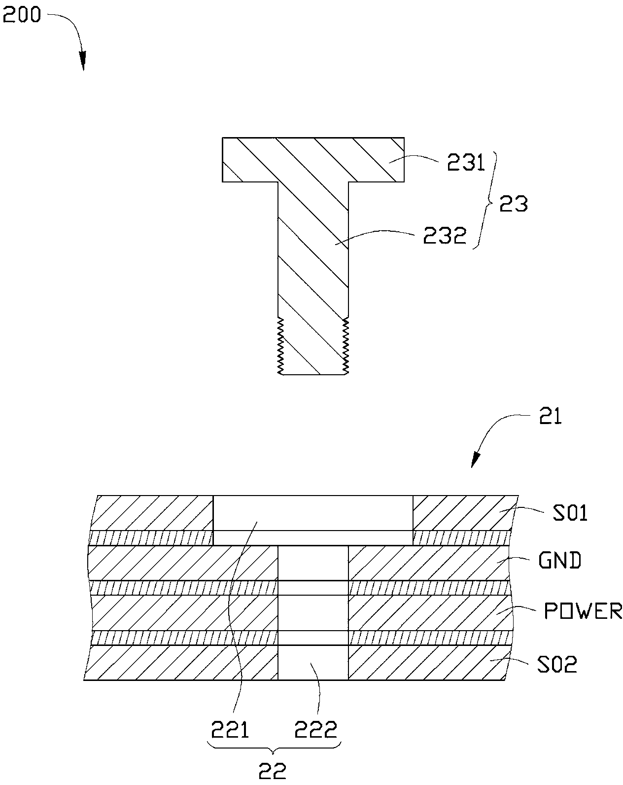
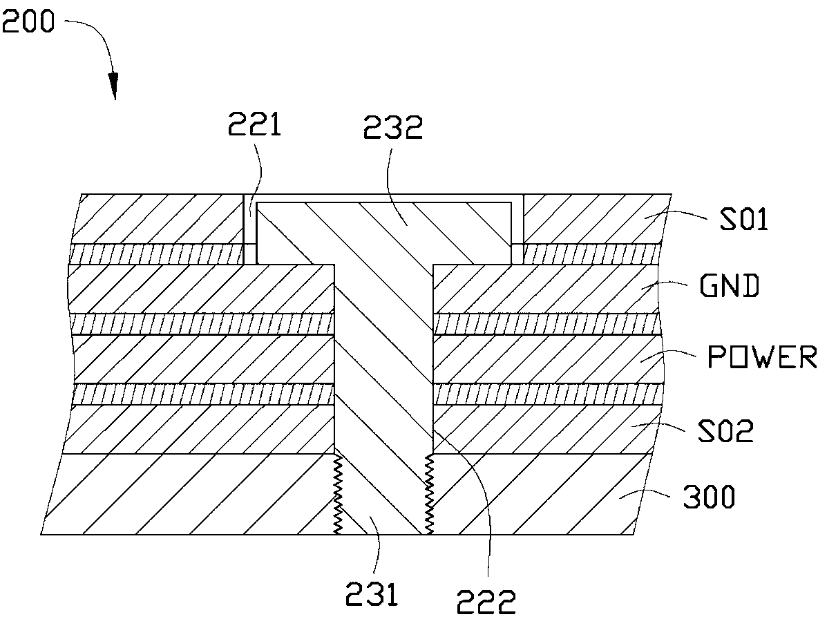
[0013] see figure 2 A preferred embodiment of the present invention provides a printed circuit board 200, which is installed in electronic devices such as computers and servers, and is fixedly connected to the grounding element of the electronic device.

[0014] The printed circuit board 200 includes a board body 21 . In this embodiment, the board body 21 is a four-layer circuit board, including a first signal layer S01 , a ground layer GND, a power layer POWER and a second signal layer S02 stacked in sequence. Wherein, a dielectric substrate (not shown) is disposed between the first signal layer S01 , the ground layer GND, the power layer POWER and the second signal layer S02 .

[0015] The board body 21 defines a through hole 22 , and the through hole 22 includes a locking hole 221 and a through hole 222 . The locking hole 221 penetrates from the top of the board 21 , that is, the first signal layer S01 to the ground layer GND. The through hole 222 penetrates from the bo...


PUM


Abstract

The invention provides a printed circuit board. The printed circuit board comprises a board body and bolts, wherein each of the bolts comprises a cap part and a rod part, the board body comprises a first signal layer, a grounding layer, a power source layer and a second signal layer, the first signal layer, the grounding layer, the power source layer and the second signal layer are sequentially arranged in a stack mode, a through hole is formed in the board body, the through hole comprises a locking hole and a penetrating hole, the locking hole is communicated from the first signal layer to the grounding layer, the penetrating hole is communicated from the second signal layer to the grounding layer and communicated with the locking hole, the cap part is accommodated in the locking part and contacted with the grounding layer, and the rod part is arranged in the penetrating hole in a penetrating mode. According to the printed circuit board, manufacture cost is low, and the ability of anti-electromagnetic interference of the printed circuit board can be effectively improved.

Description

technical field [0001] The invention relates to a printed circuit board, in particular to a printed circuit board which can effectively reduce electromagnetic interference. Background technique [0002] When the printed circuit board is in use, because the various electronic components may interfere with each other on the electrical signal, it often generates a large amount of broadband noise or noise, which seriously affects the function of the printed circuit board. This phenomenon is generally called electromagnetic Interference (electro magnetic interference, EMI). [0003] In order to reduce the electromagnetic interference generated by the printed circuit board during use, it is usually necessary to ground the current that causes the electromagnetic interference. see figure 1 , an existing printed circuit board 100 generally has a four-layer design, including a first signal layer 11 , a ground layer 12 , a power layer 13 and a second signal layer 14 . The printed ci...

Claims


Application Information

Patent Timeline
Patent Type & Authority Applications(China)
IPC IPC(8): H05K1/02H05K9/00
CPCH05K1/0215H05K2201/09845H05K2201/10409
Inventor 李磊
Owner HONG FU JIN PRECISION IND (SHENZHEN) CO LTD
Why Eureka
Try Eureka