Method for producing silicon microneedle arrays with holes and microneedle array
A microneedle array and microneedle technology, applied in the field of microneedle arrays, can solve problems such as high cost
- Summary
- Abstract
- Description
- Claims
- Application Information
AI Technical Summary
Problems solved by technology
Method used
Image
Examples
Embodiment Construction
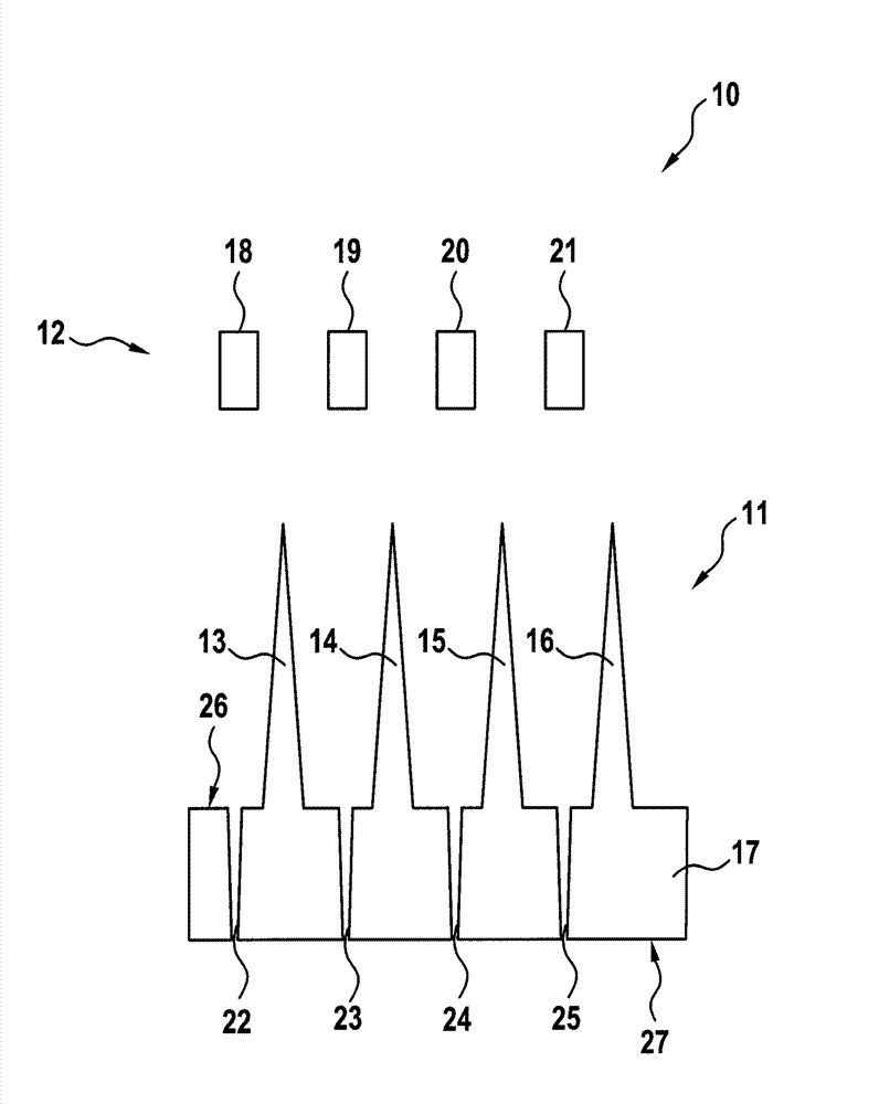
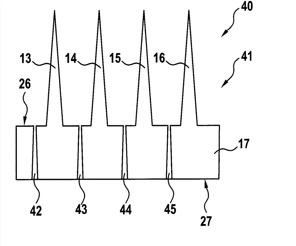
[0032] FIG. 1 shows an arrangement scheme 10 with the positions of the silicon needle array 11 and the laser lens 12. The silicon needle array 11 has needles 13, 14, 15, and 16 on a substrate 17. The laser positions 18, 19, 20, 21 are assigned to the needles 13, 14, 15, 16, respectively. Here, the laser positions 18, 19, 20, 21 are arranged on the side above the needles 13, 14, 15, 16. Using this arrangement 10 of the laser positions 18, 19, 20, 21 on the upper side of the needles 13, 14, 15, 16 to form holes in the substrate 17 from the needle side of the silicon needle array 11, that is, the front side 26 22, 23, 24, 25. In this case, the holes 22, 23, 24, and 25 in the substrate 17 are through holes, and the through holes fluidly connect the front surface 26 of the silicon needle array 11 to its flat side, that is, the back surface 27. The holes 22, 23, 24, 25 are wider on the front side 26 of the silicon needle array 11 than on the back side 27.
[0033] The laser positio...
PUM
| Property | Measurement | Unit |
|---|---|---|
| length | aaaaa | aaaaa |
Abstract
Description
Claims
Application Information


