

Display and electronic unit
A technology for display devices and display components, which is applied to electrical components, instruments, circuits, etc., can solve the problems of reducing output, increasing wiring short circuits, etc., reducing capacitance changes, suppressing image quality deterioration, and maintaining desired capacitance Effect
- Summary
- Abstract
- Description
- Claims
- Application Information
AI Technical Summary
Problems solved by technology
Method used
Image

Examples
no. 1 approach
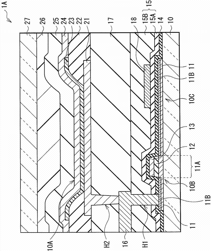
[0044] figure 1 The cross-sectional configuration of the display (organic EL display 1A) according to the first embodiment of the present disclosure is shown. The organic EL display 1A includes, for example, a plurality of pixels (organic EL devices 10A) driven by an active matrix driving method. By the way, figure 1 Only the area corresponding to one pixel (sub-pixel) is shown. In the organic EL display 1A, for example, the transistor 10B and the holding capacitor 10C sharing the oxide semiconductor film 11 are provided on the drive side substrate 10, and the organic EL device 10A is provided on a layer above the transistor 10B and the holding capacitor 10C. The emission system of the organic EL display 1A may be a so-called top emission type or a bottom emission type. The detailed configuration of each of the organic EL device 10A, the transistor 10B, and the holding capacitor 10C will be described below.
[0045] [Organic EL Device 10A]
[0046] In the organic EL device 10A, ...
no. 2 approach
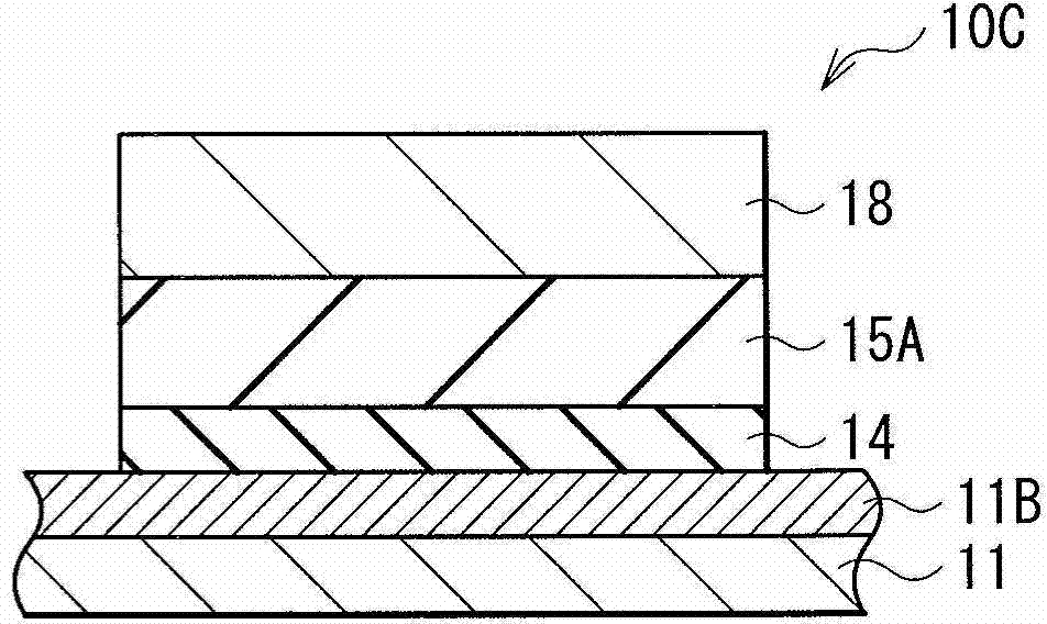
[0109] Picture 10 The cross-sectional configuration of the display (organic EL display 1B) according to the second embodiment of the present disclosure is shown. In the organic EL display 1B, the conductive film 18 configuring the upper electrode of the holding capacitor 10C is formed of a transparent conductive material, thereby making the holding capacitor 10C transparent. Therefore, in the second embodiment, it is allowed to configure a transparent display that has high transparency to visible light and emits light to the upper and lower surfaces. The transparent display is used to display the back of the display through the display, and the displayed image appears in the air, and advantageously provides a greatly improved design. The transparent display can be applied to displays for advertising and commercial purposes, such as vending machines and refrigerators.
[0110] As the transparent conductive material of the conductive film 18, a metal having high transparency to v...
Deformed example 1
[0113] Picture 11 The cross-sectional configuration of the display (liquid crystal display 2) according to Modification 1 of the present disclosure is shown. Instead of the organic EL device, the liquid crystal display 2 includes a liquid crystal device 30A as a display device. Specifically, in the liquid crystal display 2, the transistor 10B and the holding capacitor 10C are provided on the drive side substrate 10, and the liquid crystal display device 30A is provided on a layer above the transistor 10B and the holding capacitor 10C. Except for this point, the liquid crystal display 2 of Modification 1 has a configuration, function, and effect similar to those of the first or second embodiment. Therefore, the components corresponding to the components in the first or second embodiment will be described using the same symbols.
[0114] The driving side substrate 10 and the transistor 10B are configured similarly to the first embodiment. The holding capacitor 10C is configured ...
PUM
 Abstract
Description
Claims
Application Information