Silicon Oxide Nitride Oxide Semiconductor (SONOS) memory

A memory and storage unit technology, applied in the direction of electric solid-state devices, semiconductor devices, electrical components, etc., can solve problems such as user inconvenience and data loss, and achieve the effect of improving work speed

Active Publication Date: 2013-06-26
SHANGHAI HUAHONG GRACE SEMICON MFG CORP
View PDF2 Cites 0 Cited by
  • Summary
  • Abstract
  • Description
  • Claims
  • Application Information

AI Technical Summary

Problems solved by technology

However, SRAM will lose the saved data after power failure, which will cause inconvenience to users.

Method used


Image

  • Silicon Oxide Nitride Oxide Semiconductor (SONOS) memory
  • Silicon Oxide Nitride Oxide Semiconductor (SONOS) memory
  • Silicon Oxide Nitride Oxide Semiconductor (SONOS) memory

Examples


Embodiment Construction

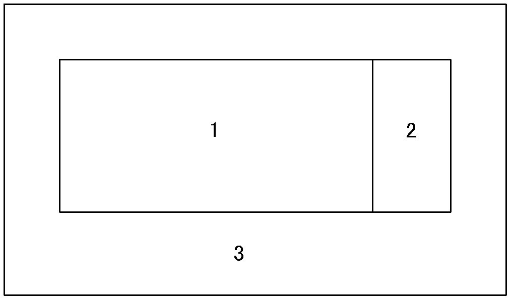
[0017] Such as figure 1 Shown is a schematic diagram of the layout of the SONOS memory according to the embodiment of the present invention. The SONOS memory in the embodiment of the present invention includes a main area 1 for data storage, a backup area 2 and a peripheral area 3 .

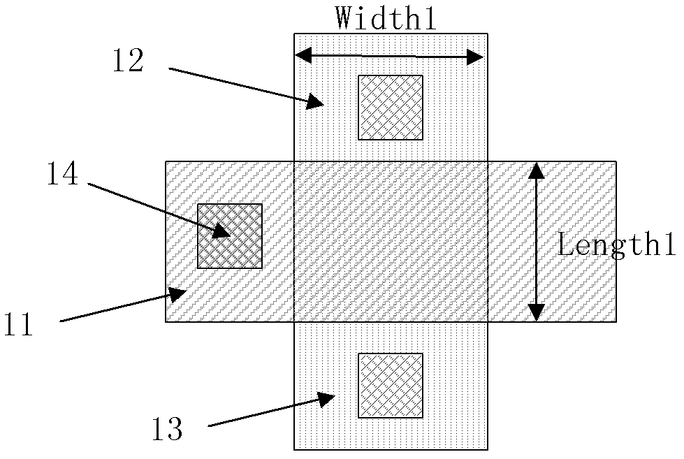
[0018] Such as figure 2 Shown is a schematic diagram of the layout of the memory cells in the main area 1 of the SONOS memory according to the embodiment of the present invention. The storage unit in the main area 1 is composed of a first SONOS transistor. The first SONOS transistor includes a gate 11 , a source region 12 and a drain region 13 , and the gate 11 , the source region 12 and the drain region 13 are respectively drawn out through metal contacts 14 . The gate 11 is connected to the word line WL, the source region 12 is connected to the source line SL, and the drain region 13 is connected to the bit line BL. The dimensions of the channel region of the first SONOS transistor include...


PUM


Abstract

The invention discloses a Silicon Oxide Nitride Oxide Semiconductor (SONOS) memory. The memory comprises a main region of data memory and a backup region of data memory. The backup region uses an SONOS transistor to be a memory unit, the size of the SONOS transistor of the backup region is increased, the working speed of the backup region is improved, the working speed of the backup region is larger than that of the main region, and quick working requirement of the backup region is met. After the backup region uses the SONOS transistor, although the size of the SONOS transistor of the backup region is increased, the SONOS transistor of the backup region can store data for days, the stored data in the backup region cannot be lost after being powered off, and a user feels convenient.

Description

technical field [0001] The invention relates to a semiconductor integrated circuit, in particular to a SONOS memory. Background technique [0002] The existing SONOS memory includes a main area for data storage, a backup area and peripheral circuits. The storage unit in the main area is composed of SONOS transistors; and the size of SONOS transistors meets the data storage characteristics of SONOS (silicon-silicon dioxide-silicon nitride-silicon dioxide-silicon) transistors for more than 10 years, due to the long data storage time , SONOS transistor erase time must be long enough such as 2 milliseconds. The backup area is used for temporary storage of data, and requires fast working speed. The storage unit of the backup area of ​​the existing device adopts Static Random Access Memory (SRAM), and the use of SRAM in the backup area can ensure that the backup area has a faster working speed . However, the SRAM will lose the saved data after power failure, which brings inconv...

Claims


Application Information

Patent Timeline
Patent Type & Authority Applications(China)
IPC IPC(8): H01L27/115H01L29/792
Inventor 陈广龙谭颖
Owner SHANGHAI HUAHONG GRACE SEMICON MFG CORP
Why Eureka
Try Eureka