Metal half hole molding method and manufacture method of printed circuit board

A printed circuit board and hole forming technology, which is applied in the direction of printed circuit manufacturing, printed circuit, and electrical connection formation of printed components, can solve problems such as failure to reach, achieve the effect of improving forming quality and overcoming residual copper wire burrs

Inactive Publication Date: 2013-06-26
ZHUHAI FOUNDER TECH MULTILAYER PCB +1
View PDF4 Cites 26 Cited by
  • Summary
  • Abstract
  • Description
  • Claims
  • Application Information

AI Technical Summary

Problems solved by technology

However, if Figure 5 As shown, the inventor found that when the metal half hole < 0.5mm, V-CUT caused the quality problem of the metal half hole < 1 / 3 of the aperture, that is, the V-CUT design method caused the metal half hole ≥ 0.2mm. Require

Method used


Image

  • Metal half hole molding method and manufacture method of printed circuit board
  • Metal half hole molding method and manufacture method of printed circuit board
  • Metal half hole molding method and manufacture method of printed circuit board

Examples


Embodiment Construction

[0026] The present invention will be described in detail below with reference to the accompanying drawings and in combination with embodiments.

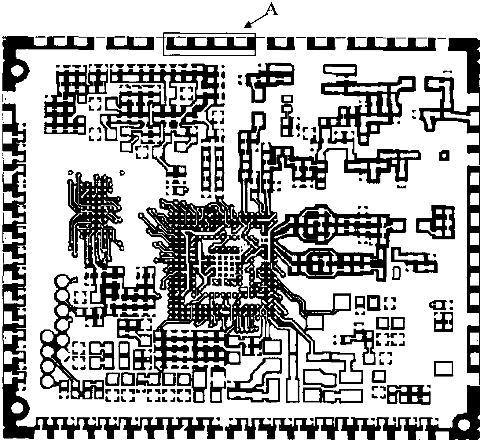
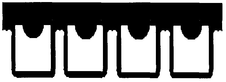
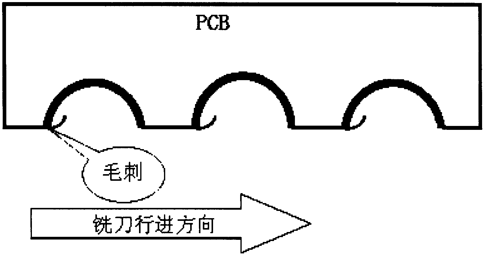
[0027] Image 6 It shows a schematic diagram of forming a metal half hole in the milling process according to an embodiment of the present invention. In the process of manufacturing a PCB, before the film removal / alkaline etching / soldering process, the printed circuit board is formed through the process of milling metal half hole.

[0028] The related technology is to form the metal half hole at the same time when the milling board is forming the shape of the PCB, so the purpose of adding the second drilling process is to avoid the copper wire burr when the milling board is forming the metal half hole. In this embodiment, the process of milling the metal half hole is advanced before the film removal / alkaline etching / sn stripping process, so that the milling process can be removed by the film removal / alkaline etching / sn stripping pro...


PUM

PropertyMeasurementUnit
widthaaaaaaaaaa

Abstract

The invention provides a metal half hole molding method. A metal half hole of a printed circuit board (PCB) is molded through a board milling procedure before the procedures of film removing, alkaline etching and tin removing in the manufacture process of the PCB. A manufacture method of the PCB is further provided. The manufacture method includes the metal half hole molding method which is used for manufacturing the metal half hole of the PCB. By means of the metal half hole molding method and the manufacture method of the PCB, the metal half hole is molded by milling the board before the procedures of film removing, alkaline etching and tin removing, the problem of residual copper wire burr is solved, and the effect of improving molding quality of the metal half hole is achieved.

Description

technical field [0001] The invention relates to the field of printed circuit boards (PCBs), in particular to a metal half-hole forming method and a PCB manufacturing method. Background technique [0002] Metal half hole is also called half PTH (plating through hole, plated through hole). figure 1 It shows a PCB with metal half-holes on all four sides of the unit according to the related art, figure 2 show figure 1 An enlarged schematic view of part A in . As shown in the figure, the so-called metal half hole refers to the metallized hole (or groove) that only half is left on the edge of the PCB shape, and the other half will be milled off during the shape processing. [0003] The general mechanical processing method of circuit board forming is CNC forming machine milling. A metal half-hole forming method in the related art is to directly form metal half-holes in the process of milling the shape of the PCB after printing characters. The specific process is as follows: ...

Claims


Application Information

Patent Timeline
Patent Type & Authority Applications(China)
IPC IPC(8): H05K3/42H05K3/00
Inventor 胡永栓陈杰标
Owner ZHUHAI FOUNDER TECH MULTILAYER PCB
Why Eureka
Try Eureka