

Bigrid pixel structure array panel structure and liquid crystal display panel
An array panel and pixel structure technology, which is applied in the direction of instruments, semiconductor devices, electrical components, etc., can solve the problems that the aperture ratio and the display effect of the liquid crystal display panel cannot be taken into account at the same time, and it is in a normal state, so as to avoid the staggered transmission area and improve the opening efficiency, and the effect of reducing the space occupied by TFT
- Summary
- Abstract
- Description
- Claims
- Application Information
AI Technical Summary
Problems solved by technology
Method used
Image

Examples
Embodiment 1
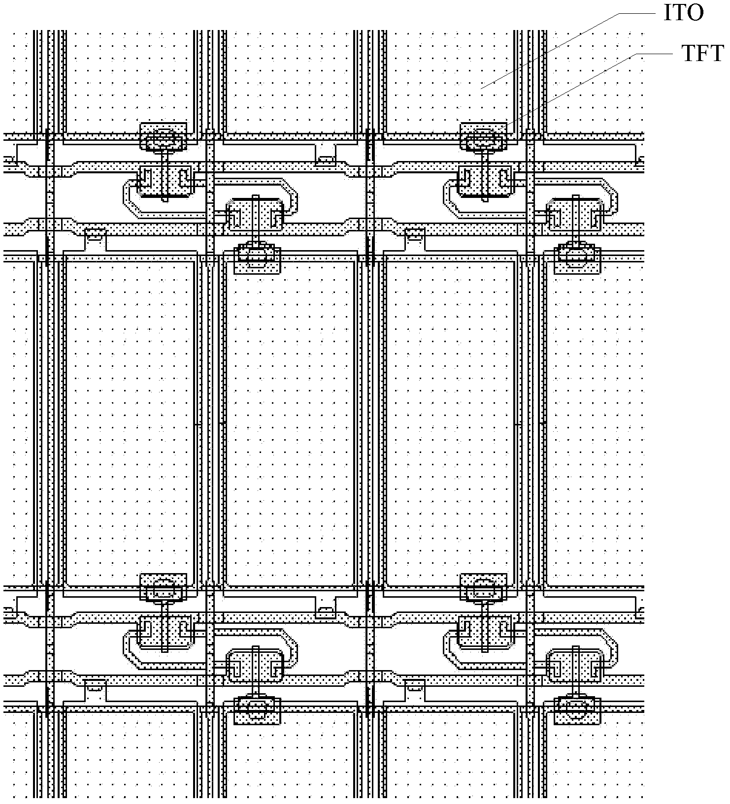
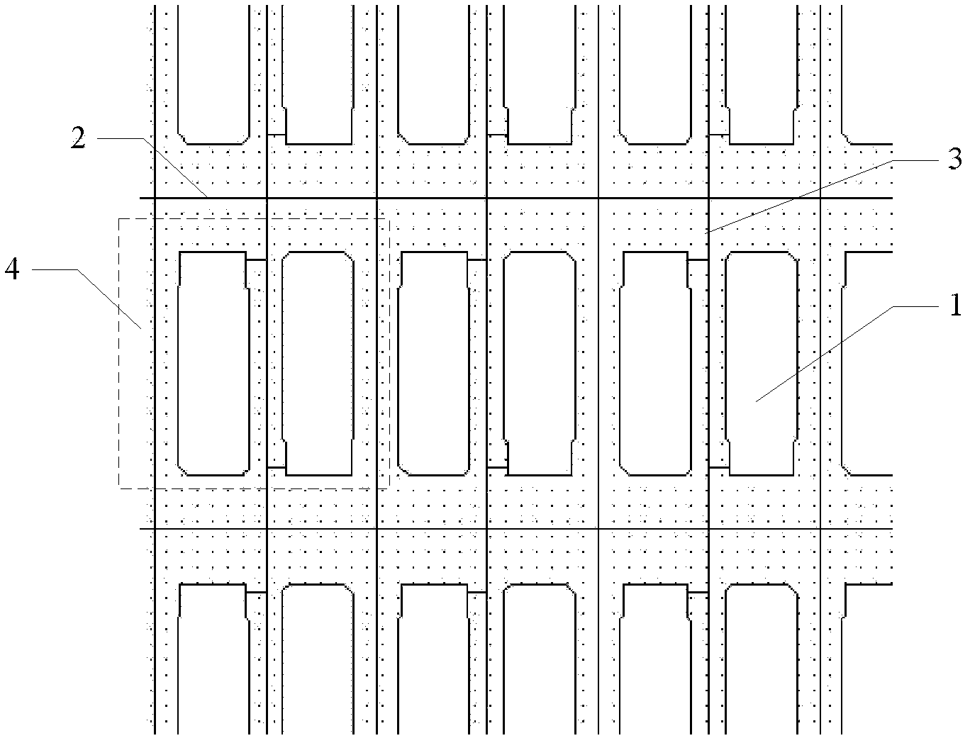
[0041] Such as image 3 As shown, it is a schematic diagram of the BM diagram of a dual-gate pixel structure array panel structure disclosed in Embodiment 1 of the present invention, which mainly includes: a glass substrate (not shown in the figure), pixel 1, and pixel electrode ITO (not shown in the figure). output), TFT (not shown in the figure), scan line 2, data line 3 and common electrode line (not shown in the figure).
[0042] A glass substrate, a plurality of scanning lines 2 and data lines 3 arranged on the glass substrate, the scanning lines 2 are arranged in rows, and the data lines 3 are arranged in columns.
[0043] A plurality of pixel regions 4 crossed by the scanning line 4 and the data line 3; wherein, one pixel region 4 includes two pixels 1, and the pixel electrode ITO of one pixel 1 is connected to one TFT, located at The centers of the pixels 1 between the two scanning lines 2 are located on the same straight line.
[0044] Two laterally adjacent pixels ...
Embodiment 2
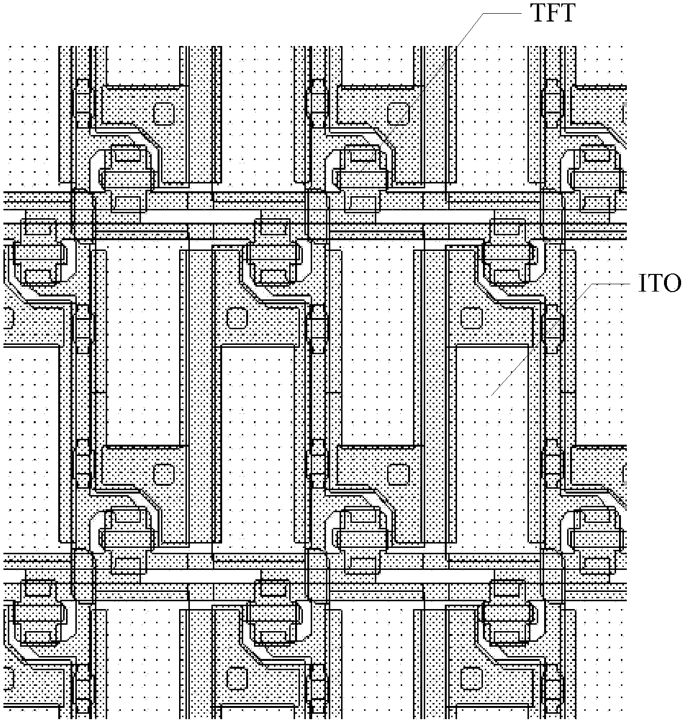
[0071] On the basis of the first embodiment of the present invention disclosed above, a common electrode line is provided between adjacent pixels connected to different data lines, that is to say, two adjacent pixels share a common electrode line, which further reduces the The area between pixels increases the aperture ratio.
[0072] At the same time, the end of the pixel electrode of each pixel that is not connected to the TFT, that is, the end opposite to the connected TFT, overlaps the adjacent scanning line by a preset length. By overlapping a certain length, the storage capacitance of the corresponding pixel is increased, and the The scanning lines at the overlap function to shield the lines, and at the same time increase the aperture ratio of the pixels. The preset length can be specifically set according to the width of the pixel or the length of the folded line of the scanning line.
[0073] Such as Figure 4 As shown, the end of the first pixel 41 that is not conne...
PUM
 Abstract
Description
Claims
Application Information