Garnet type current sensing device and manufacturing method of garnet module
A sensing device, garnet technology, applied in the direction of measuring device, voltage/current isolation, measuring current/voltage, etc., can solve problems affecting the measurement accuracy and stability of the system, complex process, high energy consumption, etc., to achieve convenience and safety Simple monitoring and system design, less optical components
- Summary
- Abstract
- Description
- Claims
- Application Information
AI Technical Summary
Problems solved by technology
Method used
Image
Examples
Embodiment 1
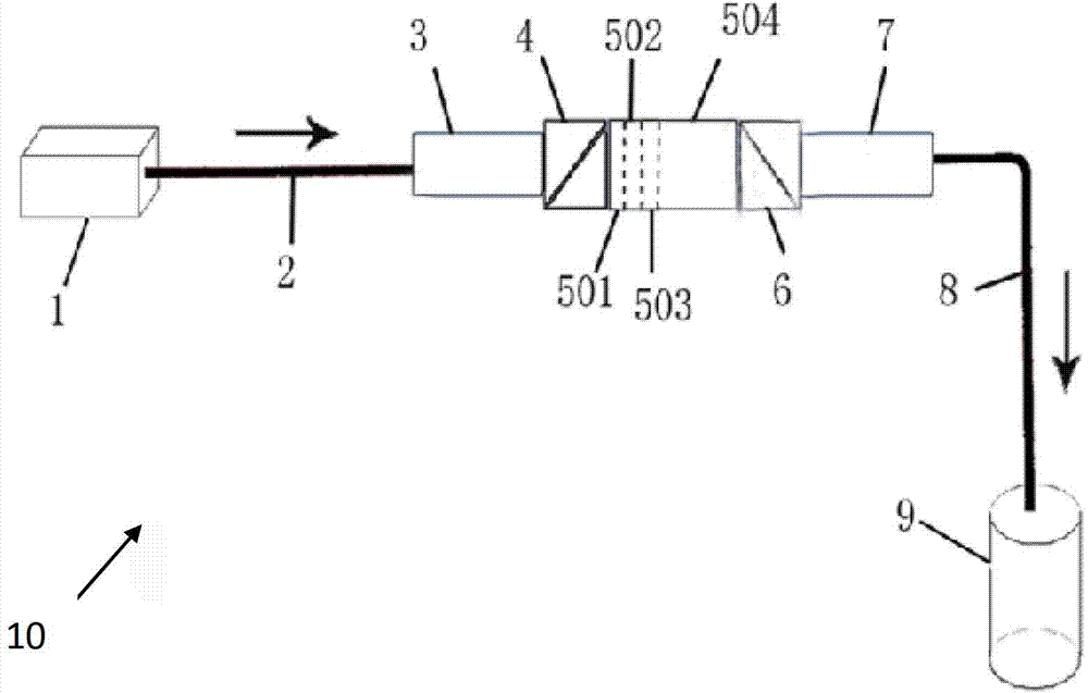
[0041] figure 1 It is a structural schematic diagram of the garnet-type current sensing device of the present invention.
[0042] like figure 1 As shown, the garnet-type current sensing device consists of a light source 1, an input polarization-maintaining fiber 2, an input fiber collimator 3, a polarizer 4, a garnet module 5, a polarizer 6, an output fiber collimator 7, an output The components such as the polarization maintaining optical fiber 8 and the detector 9 are connected in sequence to achieve a high degree of integration.
[0043] Wherein, the light source 1 is a point light source for providing a beam of natural light.
[0044] The input polarization maintaining fiber 2 is connected to the light source 1 and the input fiber collimator 3 to ensure that the polarization direction of natural light does not change when it is transmitted in the input polarization maintaining fiber 2 .
[0045] The input fiber collimator 3 is used to transform the natural light into in...
Embodiment 2
[0076] In the second embodiment, the garnet-type current sensing device can also adopt the following structure: the light source 1 can also be a surface light source. The polarizer 4 can also be a Glan polarizing prism. The buffer layer 503 is made of Ta, Ag, and Al, and has a thickness of 10 μm. The bias film layer 502 is made of neodymium iron boron (NdFeB) and samarium cobalt (SmCo) with a thickness of 7 μm. The protective layer 501 is entirely made of SiN and SiO2, and has a thickness of 80 nm. The analyzer 6 can also be a Glan polarizing prism.
[0077] In the preparation method of the garnet module 5, the thin film growth system may also be a magnetron sputtering apparatus. Other structures of the second embodiment are the same as those of the first embodiment.
Embodiment 3
[0079] In the third embodiment, the garnet-type current sensing device may also adopt the following structure: the polarizer 4 is a Glan polarizing prism. The buffer layer 503 can also be made of TAg and Al, and has a thickness of 8 μm. The bias film layer 502 is entirely made of aluminum nickel cobalt (AlNiCo) and has a thickness of 20 μm. The protective layer 501 is made of SiN, SiO2 and Ta, and has a thickness of 100 nm. The analyzer 6 can also be a Glan polarizing prism. Other structures of the third embodiment are the same as those of the first embodiment.
PUM
 Abstract
Description
Claims
Application Information

